DOI :
10.2240/azojomo0124
Nov 14 2007
Understanding basic properties of nanomaterials is crucially important for their use in nanotechnology. As one of the most widely studied materials in the last decade, carbon nanotubes (CNT) exhibit a number of interesting properties. However, widespread use of CNT in nanotechnology is hindered by intrinsic inhomogeneity of bulk synthesised material. The difficulty of separating metallic and semiconducting nanotubes from the synthesised material prevents the use of CNT in applications where identical building blocks with the same properties would be required. Another problem with the use of CNT in nanotechnology applications is their poor dispersion characteristics in low-boiling point solvents without the use of additional surfactants. These issues strongly motivate investigations of alternative nanomaterials.
One of new promising materials whose synthesis was first reported [1] in 2004, are molybdenum-sulfur-iodine nanowires. Their synthesis and preparation are much less demanding than CNTs and not surprisingly, since their discovery, the materials were researched with a wide range of techniques and have been the subject of numerous and diverse investigations, including a search for possible industrial applications. The material turned out to be a conducting one-dimensional molecular-wire-like nanomaterial which typically appears in ordered bundles[2,3] which have good dispersability in a range of common solvents [4,5], in many respects functionally very similar to CNTs. The relatively simple synthesis of the material from elements without any catalysts [1] gives a possibility for scaling production and hence applicability of the material in industrial technology. A number of possible applications are currently being pursued, ranging from molecular electronics to conducting and tribological composites.
Methods and Materials
In this article we report on collection of different investigations on basic properties of molybdenum-sulfur-iodine nanowires. The investigations range from structural studies to studies of mechanical, transport and optical properties. The structure was studied with combination of experimental techniques that included X-ray powder diffraction measurements (XRD), X-ray absorption fine structure experiments (XAFS), atomic pair distribution function analysis (PDF), high-resolution transmission electron microscopy (HRTEM) and scanning transmission electron microscopy (STEM). The experimental techniques are complemented with first principle calculations. The investigation of optical properties included measurements of reflectivity and absorbance on either mechanically orientated thin films, bulk samples or in solutions.
Nanowire Composition
The nanowires that were investigated have the chemical formula Mo6S9-xIx (3 < x < 6) and belong to a group of cluster compounds based on transition metal chalcogenides. While the clusters in most of this crystalline compounds form a three-dimensional networks, the clusters in Mo6S9-xIx (MoSIx) are arranged in one-dimensional chains. After the single step synthesis which proceeds from elements the MoSIx nanowire are usually packed in bundles, but the bundles can be controllably dispersed and were found to form a stable dispersion with individual molecular wires [5]. The MoSIx nanowires that were used in these investigations were supplied by a company Mo6 and processed by washing, dispersion and sedimentation.
Structural Properties of Nanowires
The structure of Mo6S9-xIx nanowires was first studied with X-ray diffraction [1]. It has soon become clear that other techniques or combination of techniques will be needed for detailed determination of the structure. The accurate determination of atomic occupancy of different sites from X-ray spectra was hindered, because individual nanowires are often not perfectly ordered relative to each other inside a bundle, and the bundles themselves are twisted or deformed.
The basic structure was determined by combining the local structure information from XAFS with the average structure information from X-ray powder diffraction measurements [6]. The obtained structure (figure 1) is best described in terms of a one-dimensional polymer composed of chains of covalently bound Mo-chalcogenide-halide clusters, composed of Mo6(S,I)6 units, joined together by three cations (S or I). Meden et al [6] determined the space group as P63, corresponding to the bundle structure with three parallel Mo6S3I6 wires within the unit cell. The study, which was complemented by density functional theory (DFT) calculations, also showed that there are no covalent bonds between individual nanowires, which leads to the remarkable one-dimensional properties and easy dispersion into individual molecular nanowires. This property gives rise to packing disorder when individual nanowire strands slide against each other within the bundles.
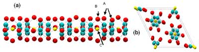
Figure 1. The atomic structure of Mo6S3I6 nanowires. (a) Side view of an individual Mo6S3I6 molecular chain with S atoms in the bridging positions B and (b) projection along the crystalline c axis. Early X-ray diffraction experiments indicated chain ordering according to the hexagonal P63 spacegroup12 (the unit cell shown with solid lines)
When the preferrential orientation of the sample in the XRD experiments was taken into account, the agreement with the model proposed by Meden et al. [6] was good enough to ascertain the backbone structure beyond any reasonable doubt, but not the occupancy of S and I on the backbone. The complementary structural study by Pair-distribution function (PDF) analysis [7] confirmed the skeletal structure, but at the same time raised some uncertainty regarding the population of S and I in the different positions. Both studies agree on presence of S in the bridging planes (positions B) and iodines for position A, but there appears to be a discrepancy regarding the occupancy of the central bridging position shown as atom C in Figure 1. Whereas the XRD shows this to be more or less unoccupied, the PDF studies suggest otherwise. This discrepancy was apparently solved by HRTEM and STEM studies, which showed no occupancy on the C site.
Structure of Self-Assembled Nanowire Crystals
HRTEM and STEM studies have been performed by Nicolosi et al. [8] on Mo6S4.5I4.5 (or 12-9-9) and Mo6S3I6 using advanced techniqes in particular annular dark field (ADF) imaging. ADF imaging using aberration-corrected STEM was used to determine the structure of self-assembled nanowire crystals very accurately particularly for Mo6S3I6. On the basis of a very detailed comparison of calculated and observed structural TEM images along different angles as shown in figure 2, the authors concluded that the packing of the nanowires has a P-1(#2) structure, rather than a R-3(#148) or P63(#173) space groups previously proposed, due to a rather subtle effect, namely the absence of a rotational symmetry along the wire, which would result in a triclinic lattice.
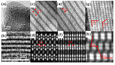
Figure 2. (a),(b) HRTEM images of bundles assembled from individual nanowires. (c)-(h) Pairs of experimental ADF STEM image (first row) and image from simulations (second row) made for three high-symmetry directions.
The authors showed that the nanowires consist of a series array of well defined unit cells each consisting of six atomic planes (see figure 3), leading to a less symmetric superstructure than originally proposed [6]. The I atoms were assigned to A sites as indicated in figure 1 while the S atoms occupy the B sites. The central bridging positions (site C) were not occupied.
![The nanowire structure of Mo6S3I6 as determined by STEM measurments [8]. The brackets define the nanowire unit cell, which containes 12 Mo (red), 6 S (yellow), 12 I (purple) atoms.](https://www.azonano.com/work/Structural%20and%20Physical%20Properties%20of%20Mo6SxI9-x%20Molecular%20Nanowires_files/image007.jpg)
Figure 3. The nanowire structure of Mo6S3I6 as determined by STEM measurments [8]. The brackets define the nanowire unit cell, which containes 12 Mo (red), 6 S (yellow), 12 I (purple) atoms.
Such a nanoscale structural determination technique was essential, since previous attempts using X-ray diffraction have proved unsuccessful and/or insufficiently accurate to determine subtle differences in occupancy of the S and I sites. The stability of structures with different stoichiometry in Mo6S9-xIx was also confirmed by density functional theory (DFT) calculations in the range of 4.5 < x < 6. Remarkably, the calculations also showed that there is very little difference in energy between the different stoichiometries (on the same backbone), indicating that S and I may interchange relatively freely, and also confirm that there are only very weak interactions between individual nanowires. The DFT calculations on the structure from Meden et al. [6] and also calculations by Tomanek et al. [10] for 12-9-9, and by Vilfan and Nicolosi et al. [9] for 636 predict the material to be a narrow-band metal along the direction of the nanowire axis, but have essentially non-metallic character for transport across the nanowires.
Summary of Physical Properties
Mechanical Properties of Nanowires
In accordance with the calculations - which showed that there are only very weak bonds between nanowire strands - MoSIx nanowires exhibit remarkably anisotropic mechanical properties. The mechanical measurements on MoSIx nanowires showed that the shear modulus was exceptionally small, on the order of 16-89 MPa, while Young’s modulus was high, up to 430 GPa [11]. The origin of these reproducible high values is not yet understood, as calculations have predicted somewhat smaller Young’s moduli, of the order of 100-150 GPa [10]. Putting these results into perspective we see that the Young’s modulus is only 2-3 times less than for the best SWCNTs, while the forces between individual nanowires are substantially weaker than in CNTs or graphite. The very small shear modulus [11,13] implies that the MoSIx nanowires are one of the best approximations to a one-dimensional material found in nature. The use of MoSIx nanowires for mechanical reinforcement in composites and reduced friction [13], stem from the large Young’s modulus and the small shear modulus respectively.
Transport Properties of Nanowires
Systematic measurements of resistivity were done both on bulk (pressed pellets) and on individual nanowire bundles [2,3]. In all cases with different MoSIx nanowires the current-voltage characteristics are linear and the temperature dependence of the resistivity was found to exponentially increase at low temperature, following variable-range hoping (VRH) behavior of the form σ =σ0 exp-(T0/T)β, where β = ¼ for pristine (unpurified) samples, and β = ½ for samples which have been annealed in vacuum at temperatures above 500 C, as shown in Figure 4. The changeover of exponent is accompanied with an increase in conductivity – suggesting that the removal of interstitial iodine increases the hole carrier concentration, resulting in higher conductivity. This change in exponent may be understood in terms of a cross-over from three-dimensional to one-dimensional VRH caused by the removal of interstitial iodine. The results conclusively show that there is a finite density of states at the Fermi energy and that the transport is dominated by incoherent hopping between states. The origin of localization is not yet understood, but the strong 1D character of the nanowires suggests that localization may occur due to defects. Indeed recent experiments have shown that improved purity of samples may give significantly higher σ0 as high as 105 S/m, while the T-dependence appears to be dependent on bundle diameter, a sign that Luttinger-liquid behaviour might be important
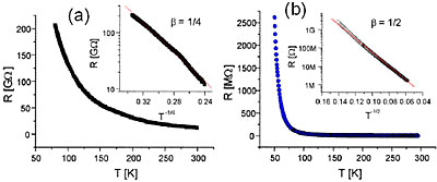
Figure 4. The resistance as a function of temperature for a Mo6S3I6 nanowire bundle measured before (a) and after (b) annealing. The insets show a log(R) versus T −1/4 for (a) and a log(R) versus T −1/2 for (b) respectively. The straight line in the inset of (a) represents a fit with β = 1/4 and 1/2 for (b) respectively
Optical Properties of Nanowires
One would expect that the 1D nature of the nanowires, which was observed by different investigations, would also show in optical properties as sharp features in optical spectra. Peculiarly no such features were observed in spite of one-dimensional character of the electronic bands and relatively sharp features in the density of states. One of the reasons for this as we found out is that there is a multitude of narrow sub-bands which belong to Mo d-derived orbitals and which lie in the region ± 2 eV from EF.
The optical absorption spectra of oriented thin film of Mo6S3I6 nanowires are shown in figure 6 (a) for E//c and E⊥c. We see a number of clear peaks for E//c and a monotonically increasing background for E⊥c. There do not appear to be any common features in the spectra, suggesting that a high degree of orientation can be achieved by the mechanical orientation process.
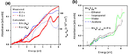
Figure 5. (a) Measurements of optical absorption in oriented thin films. The molecular axis c was in one case oriented parallel and in the other perpendicular to polarization. Solid lines are from the experiment (arbitrary scale), the other lines are calculated in the RPA. (b) The absorption spectra of Mo6S3I6 nanowires in different solvents and in addition the spectra of Mo6S4.5I4.5 nanowires in IPA.
The calculated spectra of Mo6S3I6 (also shown in the Fig 6(a)) are, like measured spectra, rather featureless below ~ 4 eV for the E | c. Above ~ 4 eV the optical transitions between the chains start to contribute. The absorption spectra for E//c show on the other hand more structure and there is quite good agreement between calculations and experiments, if calculated spectra are scaled in energy by ~1.2. The need for scaling is a consequence of the problem with DFT calculations which generally underestimates the band gap.
Absorbance spectra in solution show similar features as the dry films, except that they are hypochromically shifted by ~ 0.15 eV. In isopropanol and in water, there is an additional enhancement of the feature at around 5.5 eV (220 nm), which was suggested to arise from complexation behaviour, but its exact origin is unknown.
In Figure 6 we show the optical reflectivity measured on a pristine and an annealed pressed pellet samples of Mo6S3I6. Both show a clear plasma edge-like feature at low frequencies. The difference between the two is quite marked however, the annealed sample showing a significantly higher reflectivity than the non-annealed sample. The calculated reflectivity [also shown in Fig. 6 (a)] is substantially higher than the experimental one, in particular at low frequencies where it is dominated by the predicted metallic conductivity of the sample. This is mainly due to the large surface scattering, not fully accounted for by the data renormalization with Au-coating of our specimens. Nevertheless, the overall shape of the calculated reflectivity is similar to the measured one. Figure 6 (b) shows the real part σ1 of the optical conductivity of sample 1. The overall trend of the optical conductivity is very much indicative of a semimetal.
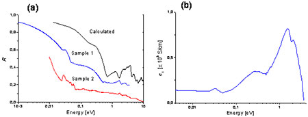
Figure 6. (a) The reflectivities R(ω) of annealed (Sample 1) and unannealed (Sample 2) samples and the calculated R(ω) for random polarizations. (b) The optical conductivity σ1(ω) of the samples 1, derived from R(ω).
Conclusions
We conclude by noting that the progress in determining basic properties of the relatively recently discovered MoSIx nanowires has been extremely rapid. Despite the difficulties in resolving nanowires structure the backbone structure has been determined with reasonable degree of accuracy. Also the characterisation experiments, which brought some surprising results, confirming the strong 1D character of MoSIx molecular nanowires. The observed properties in combination with relatively easy synthesis and dispersion make this material commercially attractive. Indeed the usefulness of MoSIx nanowires has already been investigated in areas such battery electrodes [12], tribology [12] and field emission displays [14]. The results were in general promising, but further research, particularly on growth mechanisms and stoichiometry control is needed for development of commercial products based on this material. Theoretical calculations [6,8,10,15] have been very important in determining the structure and in predicting various physical properties of MoSi nanowires. A number of theoretical predictions, particularly magnetoelasticity and electrostrictive properties are still to be investigated.
Acknowledgements
This work was supported by the EU Specific Targeted Research Project DESYGN-IT (No NMP4-CT-2004-505626).
References
- Vrbanic D., Remskar M., Jesih A., Mrzel A., Umek P., Ponikvar M., Jancar B., Meden A., Novosel B., Pejovnik S., Venturini P., Coleman J. C., Mihailovic D., “Air-stable monodispersed Mo6S3I6 nanowires”, Nanotechnology 15, pp. 635-638, 2004.
- Bercic B., Pirnat U., Kusar P., Dvorsek D., Mihailovic D., Vengust D., Podobnik B., “Transport properties of Mo6S3I6 nanowire networks”, Appl. Phys. Lett. 88, pp. 173103-1-3, 2006.
- Uplaznik M., Bercic B., Strle J., Ploscaru M., Dvorsek D., Kusar P., Devetak M., Vengust D., Podobnik B., Mihailovic D., “Conductivity of single Mo6S9-xIx molecular nanowire bundles”, Nanotechnology 17, 5142-5146, 2006. Z.Kutnjak Z et al., Two-channel electrical conduction in air-stable monodispersed MoSI nanowire sheets. J.Appl. Phys. 99, p064311, 2006
- Nicolosi V., Mccarthy D.N., Vengust D., Mihailovič D., Blau W.J., Coleman J.N., “Exfoliation of Mo6S9-xIx nanowires in common solvents”, Eur.Phys.J.Appl.Phys. 37, pp. 149 - 159, 2007.
- Nicolosi V., Vrbanič D., Mrzel A., Mccauley J., O’flaherty S., Mcguinness C., Compagnini G., Mihailović D., Werner J.B., Coleman J.N., ., “ Solubility of Mo6S4.5I4.5 Nanowires in Common Solvents: A Sedimentation Study”, J. Phys. Chem. B 109, pp. 7124-7133, 2005.
- Meden A., Kodre A., Padežnik Gomilšek J., Arčon I., Vilfan I., Vrbanič D., Mrzel A., Mihailović D., “Atomic and electronic structure of Mo6S9-xIx nanowires” Nanotechnology 16 (Bristol), pp. 1578 - 1583, 2005.
- Paglia G., Božin E. S. , Vengust D., “Accurate Structure Determination of Mo6SyIz nanowires from Atomic Pair Distribution Function ( PDF) Analysis” Chem. Mater 18, pp. 100 - 106, 2006.
- Nicolosi V., Nellist P., Sanvito S., Cosgriff E.C., Krishnamurthy S., Blau W.J., Green M., Vengust D., Dvoršek D., Mihailovič D., Compagnini G., Sloan J., Stolojan V., Carey J.D., Pennycook J., Coleman J.N.,“Observation of van der Waals driven self-assembly of MoSI nanowires into low-symmetry structure using aberration-corrected electron microscopy”, Adv. mater. 19, issue 4 (Weinh.), pp. 543 - 547, 2007.
- Vengust D., Pfuner F., Degiorgil., Vilfan I., Nicolosi V., Coleman J.N., Mihailović D., “Optical properties of Mo6S3I6 nanowires”, In Press Phys. Rev. B
- Yang T., Okano S., Berber S., Tománek D., “Interplay between Structure and Magnetism in Mo12S9I, Nanowires ”, Phys. Rev. Lett. 96,pp. 125502-1-4, 2006.
- Kis A., Csanyi G., Vrbanič D., Mrzel A., Mihailović D., Kulik A. J., Forro L., “Nanomechanical Investigation of Mo6S9_xIx Nanowire Bundles ”, Small 3, pp. 1544-1547, 2007 and Kis A., et al., “Shear and Young's moduli of MoS nanotube ropes”. Adv. Mater 15 (9), pp. 733 - 736, 2003
- Dominko R., Arcon D., Mrzel A., Zorko A., Cevc P., Venturini P., Gaberscek M., Remskar M., Mihailović D. “Dichalcogenide Nanotube Electrodes for Li-Ion Batteries”, Advanced Materials 14 (21), pp. 1531-1534, 2002.
- Joly-Pottuza L., Dassenoya F., Martina J.M., Vrbanič D., Mrzel A., Mihailović D., Vogelc W., Montagnac G., “Tribological properties of Mo–S–I nanowires as additive in oil ”, Tribology Letters 18 (3), pp. 385-393, 2005.
- Zumer M., Nemanic V., Zajec B. Remškar M., Ploscaru M., Vengust D., Mrzel A., Mihailović D., “Field emission of point-electron source Mo6S3I6 nanowires” Nanotehnology 16, 1619 - 1622 ( 2005).
- Vilfan I. and Mihailovic D., “Nonlinear elastic and mechanical properties of Mo6S3I6 nanowires.” Phys.Rev.B 74, p235411. 2006.