Sponsored by HORIBAMay 26 2008
The thin-film transistors (TFT) which drive the individual cells in the overlying liquid crystal layer in traditional active-matrix displays are formed from amorphous silicon (a-Si) deposited on a glass substrate. The advantage of using amorphous silicon is that it doesn't require high temperatures, so fairly inexpensive glass can be used as a substrate. A disadvantage is that the non-crystalline structure is a barrier to rapid electron movement, necessitating powerful driver circuitry.
It was recognized early on in flat-panel display research that a crystalline or polycrystalline (an intermediate crystalline stage comprising many small interlocked crystal) of silicon would be a much more desirable substance to use. Unfortunately, this could only be created at very high temperatures (over 1000°C), requiring the use of quartz or special glass as a substrate. However, in the late 1990s manufacturing advances allowed the development of low-temperature polysilicon (p-Si) TFT displays, formed at temperatures around 450°C. Initially, these were used extensively in devices which required only small displays, such as projectors and digital cameras.
One of the largest cost elements in a standard TFT panel is the external driver circuitry that requires a large number of external connections from the glass panel as each pixel has its own connection to the driver circuitry. This requires discrete logic chips arranged on PCBs around the periphery of the display, limiting the size of the surrounding casing. A major attraction of p-Si technology is that the increased efficiency of the transistors allows the driver circuitry and peripheral electronics to be made an integral part of the display. This considerably reduces the number of components for an individual display. The technology will yield thinner, brighter panels with better contrast ratios, and allow larger panels to be fitted into existing casings.
Experimental
The non-destructive characterizations of a-Si and Low Temperature Poly Silicon TFT-LCD panels were successfully carried out by spectroscopic ellipsometry. The ellipsometric data were collected at an angle of incidence of 70° across the spectral range 1.5-5 eV using the Horiba UVISEL spectroscopic ellipsometer.
Spectroscopic ellipsometry was used to characterize both thicknesses and optical constants of TFT-LCD devices. Moreover the grain size of p-Si materials was investigated during the study. The optical constants of silicon materials depend strongly on process conditions.
The optical properties of amorphous silicon layers are generally calculated using the Tauc Lorentz or new amorphous dispersion formula included in the materials library of the DeltaPsi2 software.
Poly crystalline layers are often modelled by a mixture of c-Si and a-Si using the Effective Medium Approximation. It allows to determine the material composition inside the layer and hence the crystallinity.
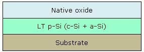
Characterization of a-Si Panels
Three layers of silicon and a top native oxide were used toion rate (HDR/LDR), and doped a-Si materials.
Figure 1. Characterization of á-Si panels
Characterization of LTPS Panels
Thickness and Optical Constants Determination
The model below was used to characterize the LTPS device. The LTPS TFT-LCD display uses the technology of laser annealing to produce highly crystalline silicon films.
Several experiments were carried out at different laser power. A shift in the optical constants was observed indicating that the crystallinity increases versus laser power.
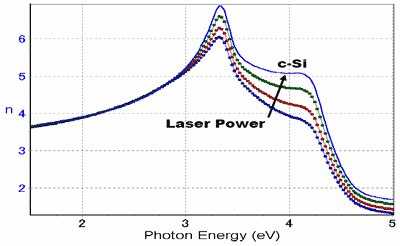
Figure 2. Illustration of laser power
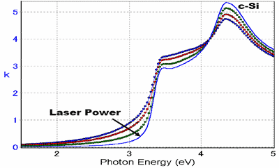
Figure 3. Illustration of laser power
Grain Size Determination of p-Si
The grain size of the p-Si can be calculated by the following formula:
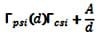
Ã: broadening parameter
d: grain size
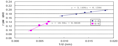
Figure 4. Broadening parameter versus inverse grain size
From this formula the nine samples processed with increasing laser power show two distinctly different curves. The blue curve represents the good process parameters for a good crystallinity of LTPS layers; the usable energy range of laser power is relatively wide. The pink curve clearly illustrates that above the optimal energy, the grain size drops sharply.
The graphics below show the excellent correlation between the Raman and spectroscopic ellipsometry techniques for characterizing the crystallinity of the samples.
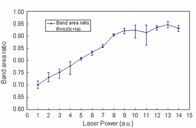
Figure 5. Band area of Raman Spectrum
describe accurately the device. The sensitivity of the ellipsometry technique allows the characterization of materials with similar optical constants (around 0.1), such as those exhibited by the high and low deposit
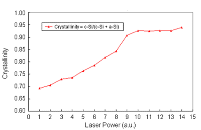
Figure 6. Crystallinity vs Laser Power
Conclusion
Spectroscopic ellipsometry is an excellent technique for the highly accurate characterization of TFT-LCD display panels based on a-Si and LTPS technologies. Owing to the sensitivity of the UVISEL spectroscopic ellipsometer and the advanced modelling features included in the DeltaPsi2 software it is possible to detect in a multistack different a-Si layers processed by various methods. Moreover the spectroscopic ellipsometry measurements allow determination of the grain size of p-Si films and illustrate the ability to characterize the crystallinity of silicon with high accuracy.

This information has been sourced, reviewed and adapted from materials provided by HORIBA.
For more information on this source, please visit HORIBA.