Since the first Nano Imprint Lithography (NIL) publications, interest in the technology has grown rapidly - starting with the scientific community and then moving to industrial sectors like integrated optics, sensors and micro fluidics.
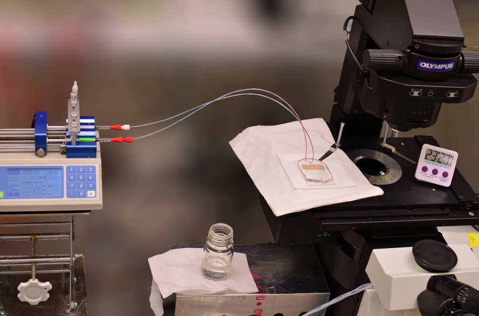
Image Credit: Shutterstock/ Rui Serra Maia
Advantages of Nanoimprint Lithography (NIL)
NIL offers several technical advantages with respect to resolution, overlay accuracy, and tool design. In addition to creating high resolution features in the nanometer range, NIL can also be employed for replicating much larger features. Presently, NIL is utilized in optical applications for the production of optical elements with feature sizes in the sub-millimeter range. With the ever increasing demand for higher integration of functionality, combined with the need to reduce structure sizes at acceptable costs, traditional lithographic techniques are fast approaching their limits. NIL is a competitive candidate for Next Generation Lithography (NGL) due to its advantages in resolution and cost effectiveness.
The potential of this technology has been acknowledged by leading experts. Subsequently, it has been added to the International Technology Roadmap for Semiconductors (ITRS) as a potential NGL solution for microelectronics at the 32 nm node and beyond.
Solution Areas for Nanoimprint Lithography from EV Group
EVG offers solutions within the three main areas of Nanoimprint Lithography (NIL):
- Hot Embossing (HE),
- UV-based Nanoimprint Lithography (UV-NIL) and
- Micro Contact Printing (µ-CP).
What is Hot Embossing?
Hot embossing technology is a low cost, flexible fabrication method, which has demonstrated polymer high aspect ratio microstructures as well as nanoimprinting patterns. It uses polymer or glass substrates to imprint structures created on a master stamp. This allows the stamp to produce many fully patterned substrates using a wide range of materials. Hot embossing is therefore suited for applications from rapid prototyping to high volume production. Hot embossing can be applied in a wide variety of fields: µTAS, microfluidics (micromixers, microreactors), microoptics (wave guides, switches) etc.
Applications of Hot Embossing
Potential Applications of Hot embossing technology include:
- Microfluidics
- Lab-on-chip Systems
- Life Sciences
- Patterned Media (HDD)
- Rapid Prototyping
Nanoimprint Lithography Systems for Hot Embossing
The EVG600 Series precision alignment systems support stamp to substrate alignment for subsequent hot embossing. Stamp and substrate are brought in contact inside an EVG500 Series vacuum chamber. A precisely controlled temperature profile (typically up to 250°C, the system supports up to 650°C) and contact force sequence (up to 350kN) create an imprint of the stamp on the substrate. Imprint areas up to 200 mm in diameter with high resolution features down to 50 nm have been demonstrated on the EVG500 hot embossing systems. Typical stamps are made out of Si, SiO2 or metals (e.g. Ni). Substrates are typically polymer substrates or coated polymers on semiconductor wafers. The high temperature option enables imprinting into materials where elevated temperatures are needed (e.g. glass substrates).
.jpg)
Large area patterning of semiconducting polymers for flexible solar cell applications. Source EVG, Courtesy of IMI-CNRC
.jpg)
Large area pattern transfer on Si using NIL on the EVG520HE. Source EVG, Courtesy of IMI-CNRC
.jpg)
Imprinted substrate with submicron lines and spaces. Imprinted on EVG520HE. Source EVG, Courtesy of Bergische Universität Wuppertal
Typical Hot Embossing Process Flow
|
|
- Temperature ramp up (top/bottom heater independently controlled)
- Temperature above Tg
- Cooling down below Tg for de-embossing
- De-embossing temperature
- Imprinting force
- Evacuation (starts when stamp and substrate are separated)
Tg Glass transition temperature of polymer to be imprinted
Source: EVG.
|
Unique Features of Hot Embossing Systems from EV Group
All of EVG's hot embossing systems have both imprinting and bonding capabilities.
EVG®510HE/UV-NIL Semi-Automated Hot Embossing System
The EVG510HE can be configured as a manual hot embosser and/or UV-NIL system for R&D processes. The field proven EVG510HE system architecture provides the best capabilities for high-vacuum and high-contact force applications. With the universal embossing chamber of the EVG510HE the whole range of polymers can be structured.
.jpg)
The EVG®510HE/UV-NIL semi-automated hot embossing system. Source: EVG.
EVG®520HE Semi-Automated Hot Embossing System
The EVG520HE is designed for both micro and nanoimprinting applications. This production-proven system from EVG accepts substrates up to 200 mm and is compatible with standard semiconductor manufacturing technologies. The hot embossing system is configured with a universal embossing chamber, high-vacuum and high-contact force capabilities and can process the whole range of polymers and dedicated glass suitable for hot embossing.
.jpg)
The EVG®520HE semi-automated hot embossing system. Source: EVG.
EVG®750 Automated Hot Embossing System
The EVG750 is designed for high volume embossing and nanoimprinting applications for imprinting of spin-on layers and polymer substrates. This high throughput system is the first of its kind in the world and can be used for high volume microfluidic device fabrication.
.jpg)
The EVG®750 automated hot embossing system. Source: EVG.
This information has been sourced, reviewed and adapted from materials provided by EV Group.
For more information on this source, please visit EV Group.