Image Credit: ogwen/shutterstock.com
Two-dimensional (2D) transition metal dichalcogenides (TMDCs), which show a semiconducting band gap, have attracted a lot of attention recently due to their remarkable electronic and optical performance
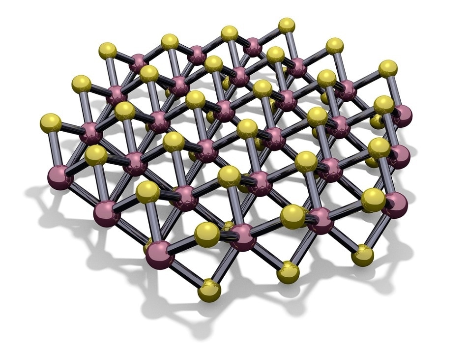
Within this, atomically thin molybdenum disulphide (MoS2) films, which have a thickness-dependent optical bandgap, have been of particular focus. A team of Researchers from South Korea have synthesized a crystalline MoS2 film from an as-sputtered amorphous film by utilizing an electron beam irradiation (EBI) process.
MoS2 films with a thickness-dependent optical bandgap range are gathering significant interest, with devices being produced for the next-generation electronic and optoelectronic applications, such as transistors, photodetectors and solar cells.
The varying bandgaps between structural forms (bulk, monolayer, alongside a quasi-particle bandgap) make MoS2 one of the most promising TMDCs for the electronic and optoelectronic industries.
However, to realize its commercial potential, a direct growth method has been required to make it compatible with conventional silicon technology and to allow its integration with flexible substrates at low temperatures.
There have been many approaches, including exfoliation, chemical vapor deposition (CVD) and physical vapor deposition (PVD), to produce wafer-scale growth of MoS2 films with the capability for commercial scale production. However, all of these processes have at least one drawback which prevents them from being a viable option for industrial scale processes.
The team of Researchers from South Korea have produced a simple method of sputtering and post-processing with electron beam irradiation (EBI). The result is a crystalline MoS2 films, which is borne out and converted from an amorphous structure, at a low processing temperature (below 100 °C).
The Researchers grew the MoS2 films using a RF magnetron sputtering system (Infovion Inc) with an attached electron beam source. The Researchers also characterized the film using a combination of high-resolution transmission electron microscopy (HR-TEM, Jeol, JEM-2100F and Jeol, JEM-4010), Raman spectroscopy (WITec, alpha 300 S), atomic force microscopy (AFM, WITec, alpha 300 S) and X-ray photoelectron spectroscopy (XPS, Ulvac-PHI, PHI 5000 VersaProbe). The Researchers also used Monte Carlo Simulations to interpret the penetration behavior of electrons in the films and investigate the atomic rearrangement in the amorphous structure.
 Interested in Equipment Referenced? Request Further Information
The EBI process only took 1 minute of irradiation (1 kV of energy) to form the crystallized 2D layered structure, which possessed a hexagonal atomic arrangement on the surface and a thickness of around 4 nm. The energy usage in this process is much lower than has previously been published, which requires between several hundred kilovolts and several megavolts to facilitate an amorphous to crystalline transformation.
The EBI process stimulated the transformation from a thermodynamically unstable amorphous structure to a stable crystalline nature with a nanometer grain size. Because of its compatibility with PVD techniques, such as sputtering and evaporation, it is thought that the processing of these MoS2 films is easily scalable and therefore carries commercial potential.
The 1 kV energy during the sputtering was enough to break down the Mo-S bond in the amorphous solid. The bond breaking process in the amorphous MoS2 structure supplied enough energy to the neighboring atoms to stimulate a local excitation. This in turn, provoked the atomic arrangement to take place, as it lowered their energies and the crystal-like bonding configurations were much more stable.
It was deduced that the incident electron energy of the EBI process was the most dominant factor in determining the crystallization pathway. The other parameters, such as the irradiation time and substrate heating, required optimization so that the damage to the sample was minimized and the crystallinity of the MoS2 thin film was maximized.
The Researchers also performed Monte Carlo simulations in order to calculate the penetration depth of electrons in the MoS2 films and to investigate the atomic rearrangement in the amorphous MoS2 structure. The full-width half maximum (FWHM) were found to be comparable to MoS2 films grown at higher temperatures and possessed an electron penetration depth of 6.9 nm.
Aside from being viable from a commercial standpoint, this novel method could easily be applied to grow other TMDCs such as MoSe2, WS2, and WSe2. It is a promising approach for realizing low-cost and low-temperature applications which are based on flexible platforms, such as various sensors, photodetectors and transistors.
Sources and Further Reading
- “Atomic rearrangement of a sputtered MoS2 film from amorphous to a 2D layered structure by electron beam irradiation”- Kim B. H., et al, Scientific Reports, 2017, DOI:10.1038/s41598-017-04222-6

This information has been sourced, reviewed and adapted from materials provided by WITec GmbH.
For more information on this source, please visit WITec GmbH.
Disclaimer: The views expressed here are those of the author expressed in their private capacity and do not necessarily represent the views of AZoM.com Limited T/A AZoNetwork the owner and operator of this website. This disclaimer forms part of the Terms and conditions of use of this website.