The ELPHY MultiBeam from Raith sets a new commercial standard for SEM and FIB-SEM nanolithography solutions. It integrates the newest technology for 3D ion beam based nanofabrication and other 3D nanofabrication methods with the superior EBL performance, and helps to unlock the total nanofabrication potential of a FIB-SEM, SEM or HIM system.
The ELPHY MultiBeam includes full multiple method nanopatterning functionality in a single tool for Focused Ion Beam Nanofabrication, Etching and Deposition, Electron Beam Lithography (EBL), Helium Ion Beam Patterning and Gas assisted Focused Electron Beam Induced Processing (FEBIP).
ELPHY MultiBeam Product Details
Main Application
- SEM lithography
- Nanolithography
- FIB-SEM nanolithography and nanopatterning
- (3D) rapid nano prototyping
- Helium Ion Microscopy - HIM - lithography
Attachment
- Attach to analytical FIB-SEM, SEM, or HIM supplier instrumentation
Stage
- Depends on analytical SEM, FIB-SEM or HIM supplier
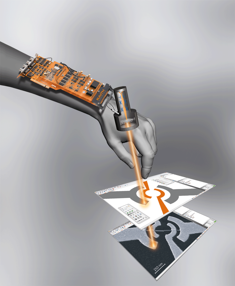
Nanolithography “pen” – ELPHY turns your SEM or FIB-SEM into a nanofabrication system. Image credit: Raith
Undreamt-of Possibilities
- Full on-site system installation and training
- Free of charge global support infrastructure for broadest range of nanofabrication and nanolithography applications
- Easy to use, fully integrated Raith NanoSuite software
- Flexible upgrade (trade-in) concept with access to complete Raith product line
- True multi user management by user authentication and related specific system parameter administration; Users find their system as they have left it
- Maximum-speed 20 MHz dual DAC addressing for X and Y main beam deflection (16 bit) with low noise differential outputs
- Accurate six extra multiplying 16-bit DACs for multilevel lithography, maximum precision overlay alignment, and write field calibration with sub-nm step size control
- Separate thermo-stabilized and RF-shielded 19” electronic unit with DSP technology supplying ultimate performance regarding highest precision, lowest noise and long term stability enabling complex applications
- Multi I/O Signal Router with touch screen display for convenient automatic or manual signal switching between ELPHY and other auxiliaries sharing same external scan input as EDX/WDX/…
- FLEXposure directional scanning modes, flexible patterning attributes manager, recipe manager and GDSII patterning-on-image (POI) functionality
- Dedicated NanoPECS Proximity Effect Correction and advanced 3D-Lithography software modules, test samples, calibration standards, starter kits and additional accessories available
Relying on Field Proven Technology and Being Prepared for the Future
The ELPHY nanolithography and nanofabrication upgrade kits are the ideal, most flexible and cost-effective solution for entering the Electron and Ion Beam Lithography world by speeding up SEM, FIB-SEM and HIM. With a track record of around ~1000 installations, ELPHY is the most extensively distributed SEM/FIB lithography attachment in the market. Raith Nanosuite software is integrated into ELPHY as well as into full Raith systems, process compatibility is maintained and upgrading made easy.
ELPHY MultiBeam Applications
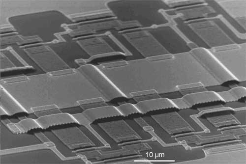
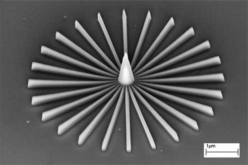
DEMUX device - J. Degenhardt, University of Duisburg, Germany
Quantum effect device - A. Nadzeyka, customer demo Raith @ Zeiss
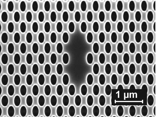
Inner part of photonic crystal with defect
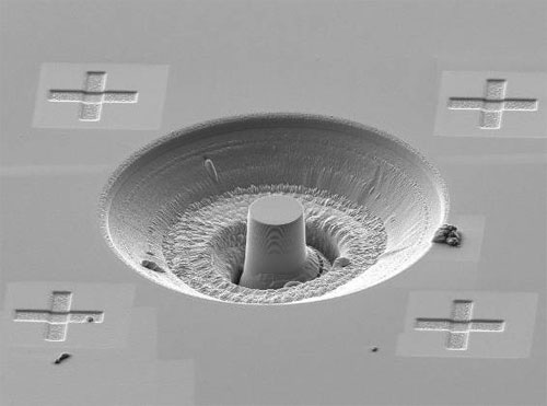
Nano mechanical resonator for sensing applications - M.Ali, UAlberta, CA
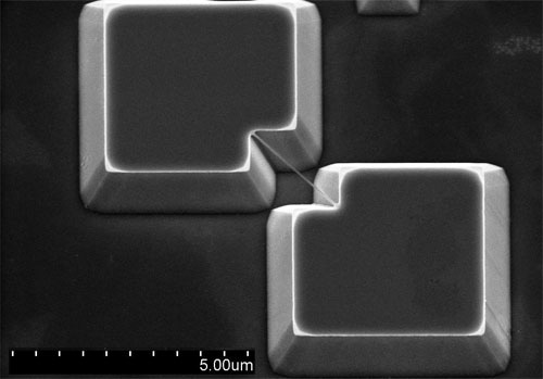
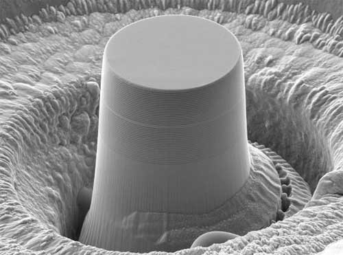
Prototyping of optical resonators - F. Pérez-Willard
Insulator deposition for growth rate studies - S. Bauerdick, Raith GmbH
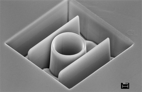
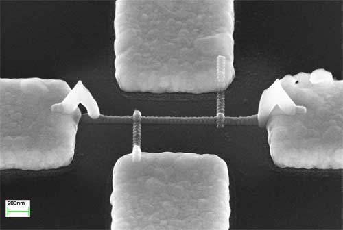
Conductive 3D deposition for optimized contact resistance - S. Bauerdick, G. Piaszenski, Raith GmbH
Prototyping of optical resonators - F. Pérez-Willard