Large-area, ultra-high-resolution 3D SEM imaging applications in chip reverse engineering, life sciences (e.g. connectomics) and materials science require surfaces of up to cm² areas to be scanned with nanometer resolution and exceptional layer to layer accuracy (‘3D stitching’) for schematic and layout extraction or 3D modeling. Traditional SEM instruments are fundamentally limited by small, uncalibrated fields of view (FOVs) and inexact sample positioning. The CHIPSCANNER, on the other hand, addresses these challenges by integrating the flexibility and resolution of an SEM instrument with the stability, accuracy and automation of an electron beam lithography (EBL) instrument. High-resolution, large-area image mosaics are formed by capturing sequential SEM images and stitching them together for additional analysis, while the laser interferometer stage and field-of-view calibration minimize overlap and concomitant computing.
With its unique blend of high-resolution SEM imaging, laser interferometer stage positioning, multiple electron detectors and FOV calibration, CHIPSCANNER creates the most accurate large-area, high-resolution images directly taken by an SEM instrument. Since the absolute position of each pixel even over cm² is eventually known to the accuracy afforded by the laser interferometer stage, these images can be stacked (3D-stitched) with the maximum possible accuracy.
CHIPSCANNER Product Details
Main Application
- Anti counterfeiting analysis
- Chip design recovery
- IP protection
- Layout reconstruction
- Chip obsolescence management
Column Technology
- Gemini
- 30 kV
- Electron
- Inlense SE detector
- Inlense BSE detector option
Stage
True large-area SEM: The laser interferometer stage and field-of-view correction minimizes overlap and concomitant computing resulting in higher stability and better results. Image credit: Raith
- Minimum image overlap
- Calibrated images
- Superior layer to layer accuracy (laser interferometer controlled stage)
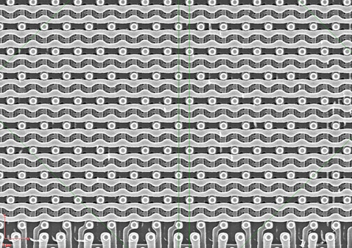
Large-area Image Mosaics with Highest Stitching Accuracy
Calibrated image scans of up to 50,000 x 50,000 pixels reduce the number of images and seams while still reducing pixel sizes. Sample pre-leveling technologies, height-sensor-based focus correction and integral temperature stabilization (optional) deliver homogenous large-area image mosaics with least stitching errors. The very high beam current stability additionally supplies very stable brightness/contrast values. Finally, the ultra-high performance at low kV allows imaging of both sensitive biological samples and charging semiconductors.
Depending on the particular stage travel range, multiple samples can be loaded and image mosaics can automatically be derived without user interaction. Software tools are available to extract and enhance valuable GDSII-CAD data from the images for additional semiconductor processing.
With its stability, high accuracy and resolution, CHIPSCANNER is the ideal large-area imaging SEM solution whenever a high-resolution SEM image analysis of large areas is desired, for instance in biological applications such as brain mapping or IC reverse engineering applications.
CHIPSCANNER Applications
5 by 5 SEM images (30 µm field of view each) of a DRAM device displayed using mosaic functionality for IC reverse engineering
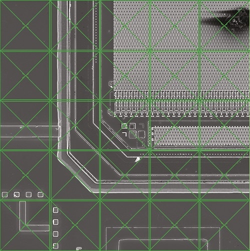
Zoom into image data (left) at higher resolution showing the negligible stitching error indicated by the green vertical line
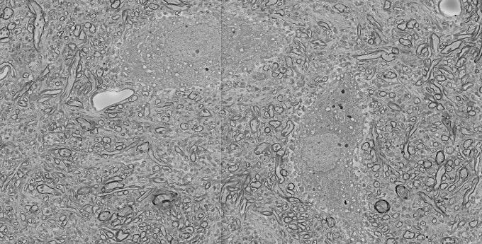
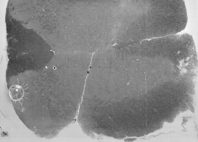
A 1.6 mm x 0.7 mm large area cross section of spinal cord with high-resolution images extracted, captured with 100 µm x 100 µm corrected FOVs (Image Credts: George Washington University)
Section of motor neurons of the same spinal cord (Image Credits: George Washington University)