SUSS MicroTec (FWB:SMH)(GER:SMH), a leading supplier of process and test solutions for semiconductor industry and related markets, announces the release of the probe station PA300PS 3D geared for 300mm electrical probing of 3D stacked structures on wafer level and targeted at the market for 3D integration. The flexible probe station allows for various engineering and monitoring tests after wafer production as well as before further stacking steps or final packaging. With the launch of the new tool SUSS MicroTec supplements its product suite of wafer bonders and lithography equipment for 3D integration.
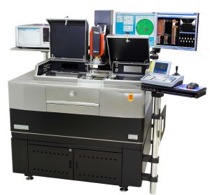 PA300PS 3D: the worlds first probe station for electrical probing of 3D stacked structures (Photo: Business Wire)
The new PA300PS 3D meets critical test challenges with MicroAlignTM, a special alignment function for vertical probe card technologies, with Automated Thermal Management (ATMTM), a system for active thermal compensation at various test temperatures, and a unique mechanical stability of the chuck system that renders it possible to introduce SUSS MicroTec’s high performance tests in 3D testing environments. The functionalities enable a wide temperature range and allow collection of low signal data in an environment free from electromagnetic interference (EMI) via ProbeShield Technology. Using high pin count vertical probe cards, in combination with MicroAlignTM technology, enables damage free probing of small test pads and minimizes pad probe marks.
Micrometer resolution is guaranteed by the newly developed z-theta chuck stage assembly also achieving increased thermal and mechanical stability for high accuracy, low drift and maximum stiffness at high probe forces. The thermal chuck system together with adjustable probe card levelling provides the highest planarity and fastest temperature transmission time on the market thus securing high test effectivity. For maximum operations safety and efficiency the PA300PS 3D additionally offers ContactViewTM technology and iVistaTM microscope visualization of all ongoing tasks in 3D applications.
“The roadmap of SUSS MicroTec’s Test division clearly meets the industry’s demands for a test solution for 3D integration”, explains Wilfried Bair, VP Business Development SUSS MicroTec.
“I am proud that this new testing capability rounds off our product offerings in 3D integration. This allows us not only to offer an almost complete product suite from one single source to our customers but also to continue to push technology development that addresses present and future needs of our customers.