Mar 17 2010
Economy and information society are dependent on rapid internet communication. The encoded data rushes through optical fibers in the form of light, but they are still processed electronically. This transition costs time and energy. The SOFI project coordinated by KIT scientists therefore aims at integrating the optics on the same type of chip that has been used in the electronic semiconductor industry for a long time already. The EU funds this project of seven partners with a total of 2.5 million euros under the 7th Framework Programme.
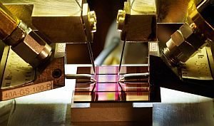 Test of a silicon chip with thousands of optical modulators contacted with high-speed electrodes and glass fibers (from above). (Photo: Hardy Müller)
The SOFI (Silicon-organic Hybrid Fabrication Platform for Integrated Circuits) project that started in January this year is aimed at producing optical waveguides and electro-optical modulators based on silicon by employing a method suitable for mass production. Due to the miniaturization achieved with the silicon waveguides, the amplification effort of electric signals can be reduced and, thus, power consumption decreased. By increasing the modulation speed, operators of telecommunication systems can also transmit more data via a glass fiber. No additional cables are required. The design developed by the KIT Institute for Photonics and Quantum Electronics (IPQ) under the direction of Professor Dr. Juerg Leuthold allows to expect “a transmission rate of more than 100 gigabits per second, which is twice the value reached today by comparable technologies, while energy consumption is reduced to five femtojoules per bit only”. This is about 1000 times less energy than needed in today’s systems.
Worldwide, researchers are working actively on combining optics and electronics on a single chip. The thus improved energy efficiency is highly welcome. Carbon dioxide emission of information and communication industry alone amounts to 2%, according to calculations made by Gartner. Furthermore it was found by a Fraunhofer study that production and use of information and telecommunication systems consume about 10% of the electricity in Germany, with increasing tendency due to booming internet communication.
“To encode data on a light signal, you can simply switch on and off a laser diode, but this is not the fastest option”, explains Dietmar Korn, a member of Professor Leuthold’s team. “Instead, we modulate the phase of the light after it has left the source.” The trick: If light propagates through certain crystals and an electric field is applied, the refractive index of the material is changed. The speed of light can be manipulated and its phase modulated. Optical chips may be applied in fields other than telecommunication. E.g., instead of linking gigantic computer complexes by copper cables, optoelectronics may be used with reduced energy consumption.
The EU project pursues both a pragmatic and ambitious approach. “We take the principle that works well with expensive lithium niobate and transfer it to inexpensive silicon”, explains Leuthold. “Silicon has a high refractive index which allows to confine light to smaller waveguide structures, as a result of which more components can be realized on the same chip.” And it consumes very little energy, because the electrodes are brought very closely to the waveguides and can be controlled with very little voltage. The electronic signal does no longer need any amplification. With a single silicon modulator, a bandwidth of 100 gigahertz shall be reached. To further increase the transmission rate, several modulators are connected in a complex circuit.
Chips guiding light require special wafers of silicon with an intermediate oxide layer. Various organic materials have to be studied for their suitability. The chips are structured by the Belgian institute IMEC using technology ready for mass production. Due to their promising materials, Rainbow Photonics, CUDOS, and GigOptix-Helix are project partners. The Italian group Selex Sistemi Integrati represents the user side and the Greek research laboratory AIT studies application scenarios. “The EU only funds research that has a permanent effect”, underlines project coordinator Leuthold. “The AIT therefore designs scenarios as to how components with different properties shall be combined and which specifications have to be obeyed”.
In addition to administration, IPQ is also responsible for the design of the light circuits. Moreover, components produced as a result of the research process are measured and evaluated. Some of the chips will be tested under application conditions at the systems laboratory of IPQ and, hence, compete in the hunt for the world record in transmission rates.
According to Professor Leuthold, there are three reasons why SOFI will be successful in the design and implementation of ultra-fast and energy-efficient modulators. “First, we are highly motivated, because we are aware of the importance of our work. Secondly, the project profits from many years of preparation work. And thirdly, the consortium combines the critical mass of expertise required for a breakthrough.”