The April issue of the premier scientific magazine Nature Photonics publishes the first experimental proof of all-optical ultra-fast communication signal processing with silicon-based devices for transmission speeds above 100Gbit/s. The paper results from the collaboration between University of Karlsruhe, Germany; IMEC, Leuven, Belgium; Lehigh University, USA and ETH Zürich, Switzerland. The achievements are a key step towards the development of complex silicon-based photonic integrated circuits.
All-optical signal processing is particularly of interest in telecommunications applications, where speed, power and cost are crucial. A key element to enable all-optical processing is optical waveguides with highly nonlinear and ultra-fast performance. Researchers from University of Karlsruhe, IMEC and its associated laboratory INTEC at Ghent University, Lehigh University and ETH Zürich fabricated an innovative optical waveguide structure by combining deep-ultraviolet lithography, standard CMOS processing and organic molecular beam deposition. This so-called silicon-organic hybrid (SOH) approach enables the fabrication of waveguides which pave the way towards all-optical processing, where photons do no longer need to be converted to electrons. This is considered to be one of the most promising ways to handle the rapidly increasing global communication traffic.
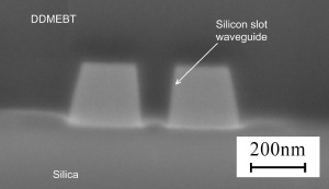
A 4mm long SOH waveguide with a record nonlinearity coefficient of ? ˜ 105(Wkm)-1 in the 1.55µm telecommunication window proved the capability of the SOH concept. As such, record values predicted by theory have for the first time been experimentally confirmed. Based on these waveguides, all-optical demultiplexing of a 170.8Gbit/s telecommunication signal to 42.7Gbit/s was performed using four-wave mixing. This is the fastest silicon photonic optical signal processing demonstrated to date. This experiment proved the viability of the SOH waveguides for all-optical processing of broadband telecommunication signals.
With the SOH approach, some inherent limitations of silicon could be overcome. Silicon-based technology, in particular silicon-on-insulator (SOI) technology, has already proven very successful for the fabrication of various passive linear optical devices such as filters. The development of ultra-fast active Si-based functionalities, such as all-optical switching, remained challenging due to the slow dynamics caused by unwanted non-linear effects in silicon. So far, the data rate achieved by using bare silicon waveguides was limited to only 40Gbit/s. The SOH approach overcomes this intrinsic limitation - thus enabling data rates above 100Gbit/s - by combining the best of two worlds: mature CMOS processing is used to fabricate the waveguide, and organic molecular beam deposition is used to cover it with organic molecules. These molecules efficiently transfer all-optical interaction without introducing significant absorption. The ability of the organic material to homogeneously fill the slot between the waveguides is a key feature of the deposition process.
The silicon circuits were designed by researchers of the University of Karlsruhe in a fabless way, and were fabricated through the ePIXfab service on IMEC's 200mm silicon photonics platform. ePIXfab (www.epixfab.eu) is a European funded initiative coordinated by IMEC to allow cost-effective fabless prototyping in wafer-scale silicon photonics technology for R&D. ePIXfab runs multi-project wafer shuttles in which designs from world-wide users share mask and processing costs.
IMEC is a world-leading independent research center in nanoelectronics and nanotechnology. IMEC vzw is headquartered in Leuven, Belgium, has a sister company in the Netherlands, IMEC-NL, offices in the US, China and Taiwan, and representatives in Japan. Its staff of more than 1650 people includes about 550 industrial residents and guest researchers. In 2008, its revenue (P&L) was estimated to EUR 270 million.
IMEC's More Moore research aims at semiconductor scaling towards sub-32nm nodes. With its More than Moore research, IMEC looks into technologies for nomadic embedded systems, wireless autonomous transducer solutions, biomedical electronics, photovoltaics, organic electronics and GaN power electronics.
IMEC's research bridges the gap between fundamental research at universities and technology development in industry. Its unique balance of processing and system know-how, intellectual property portfolio, state-of-the-art infrastructure and its strong network worldwide position IMEC as a key partner for shaping technologies for future systems.