May 26 2009
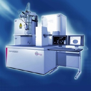
Vistec Lithography presents the latest version of its EBPG product line. Vistec's EBPG5200 features the most advanced electron beam lithography technology for exposure of substrates - from small fragments to complete 200mm substrates.

The EBPG5200: Evolution rather than Revolution:
The Vistec EBPG5200 represents the continued development stage of the successful EBPG product series. With added improvements in resolution, noise reduction, and stability, the Vistec EBPG5200 is even better adapted to the diverse and ever increasing nanotechnology requirements of science and research at universities, academic and industry-related research centers.
The Vistec EBPG5200 enables users to address a multitude of application fields, such as nanotechnology, biotechnology, integrated optics, security, semiconductor research, X-ray optics, MEMS and sensor engineering to name but a few of them. Vistec EBPG5200 system users benefit from more than thirty years of experience that Vistec has gained in the electron beam lithography business. This is clearly demonstrated by a large established base of EBPG systems currently installed worldwide.
Safe Investment for the Future:
A “modular” concept for functional features and user needs is the heart of the EBPG5200 scheme. The Vistec EBPG5200ES (Entry System) is the cost-efficient basic version of the EBPG5200 series. Upgrading to the full EBPG5200 functionality may be performed at any time, depending on the user’s available budget and application requirements. This highly flexible concept facilitates adaptation to the latest requirements and future application needs while offering various retrofit modules that are affordably priced.
Extended Platform:
The Vistec EBPG5200 is equipped with a modified platform that supports full exposure of substrates to a maximum size of 200mm. Like the previous EBPG tools, it can be used to expose fragments and special substrates in addition to standard substrate types and sizes. Essential design principles of the previous EBPG systems have been incorporated into this new 200mm platform.
Leading Edge Lithography:
With further enhancements in resolution, noise reduction and beam stability, the Vistec EBPG5200 is set to generate structures to less than 8nm on substrates of any size and type. Its electron-optical column (TFE source) is rated for acceleration voltages of 20, 50, and 100kV. With the EBPG5200 Vistec offers true 100kV / 1mm performance under regular electron-optical conditions.
However, what makes Vistec’s electron beam lithography of superior standards actually possible is the perfect match of the various system components such as the electron-optical column, the hardware platform, the data processor and the exposure engine working together in a flexible and user friendly system.
One example, how this relates to practice is the structuring of fine gates and coarser connector pads in transistor arrays. By splitting the job into a coarse and fine writing strategy, throughput can be maximized. Such sub-50nm gates can be structured to run at optimum exposure current and the coarser pads exposed with a useful beam current greater than 100nA and a maximum deflection rate of 50MHz in an automatic exposure cycle. Switching between ultra-high resolution and throughput occurs on a floating basis and is fully automated. No manual intervention is required, whether at the electron-optical column or in terms of program sequence.
Simple Operation – Highest Fexibility:
The system incorporates an interactive graphical user interface (GUI) that provides the ease of use for diverse “multi user environments”, as often required in the case of large user teams. The EBPG5200 has a proven and reliable load-lock. With a maximum holding capacity of ten equal or different substrate holders, the load-lock can accomodate a variety of substrate sizes and types as necessary for the particular application task. With this highly automated operation mode, users may also tailor the exposure sequencing to their specific requirements. Furthermore, the system includes LINUX based operational software and the user may choose his preferred data preparation scheme.
The EBPG5200 – The System of Choice for Electron Beam Nanolithography:
The EBPG5200 represents a high performance electron beam lithography patterning system for today’s and future nanotechnology requirements. With its evolutionary design, advanced lithography specification, performance and software, as well as with its substrate flexibility, compact footprint, and excellent global service support, the EBPG5200 is the system of choice for all current and future nanotechnology applications