Applied Materials, Inc., the global leader in Nanomanufacturing Technology™ solutions with a broad portfolio of innovative equipment, service and software products for the fabrication of semiconductor chips, flat panel displays, solar photovoltaic cells, flexible electronics and energy efficient glass, today introduced its Applied Charger™ UBM PVD system that defines a new standard in metal deposition productivity and reliability for chip packaging. Specifically designed for under-bump metallization (UBM), redistribution layer and CMOS image sensor applications, the Charger system’s new linear architecture more than doubles the wafer output of competing systems to deliver the highest productivity available. In addition, proprietary Isani™ wafer treatment technology allows the Charger UBM system to process ten times more wafers between servicing to enable best-of-breed uptime performance and the lowest available per-wafer cost.
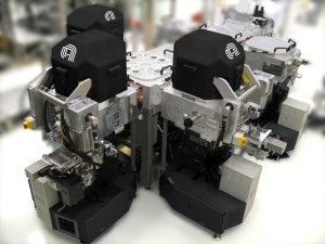 The Applied Charger system's new linear architecture more than doubles the wafer output of competing systems to deliver the highest productivity available. (Photo: Business Wire)
“Packaging facilities need a fast, dependable metallization workhorse to maximize wafer output and minimize the system redundancy burden imposed by slower, less reliable alternatives,” said Steve Ghanayem, vice president and general manager of Applied Materials’ Metal Deposition and Front End Products Business Unit. “By blending our proven PVD* process technology with packaging-specific innovations, we’ve created a highly productive, cost-efficient solution that is already churning out wafers in high volume production at multiple customers around the world.”
Key to the Charger platform’s high productivity is its streamlined modular architecture that easily expands from three to five processing stations to sequentially deposit multiple thin films while keeping the wafer in an ultra-clean, ultra-high vacuum environment. Incoming wafers are conditioned using novel Isani wafer treatment technology that ensures a low-resistance, low-contaminant interface between the incoming device and the metal films to be deposited while also delivering excellent defect performance and greatly extended maintenance intervals. Applied’s superior PVD reactor technology can tailor the properties of each film layer for optimum device performance while the flexible architecture enables extendibility to emerging three-dimensional interconnect and packaging technologies.
The Charger UBM system builds on Applied’s two decades of leadership in PVD metallization technology. Applied’s PVD systems are used by virtually all advanced manufacturers around the globe for fabricating chips. For more information, visit: https://www.appliedmaterials.com/
* PVD = physical vapor deposition