Graphene is the two-dimensional crystalline form of carbon, whose extraordinary electron mobility and other unique features hold great promise for nanoscale electronics and photonics. But there's a catch: graphene has no bandgap.
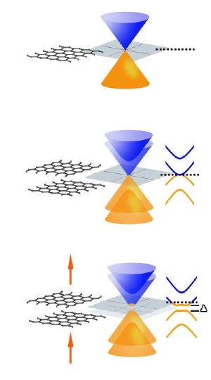 One of the most unusual features of single-layer graphene (top) is that its conical conduction and valence bands meet at a point -- it has no bandgap. Symmetrical bilayer graphene (middle) also lacks a bandgap. Electrical fields (arrows) introduce asymmetry into the bilayer structure (bottom), yielding a bandgap (Ä) that can be selectively tuned. Credit: Lawrence Berkeley National Laboratory
"Having no bandgap greatly limits graphene's uses in electronics," says Feng Wang of the U.S. Department of Energy's Lawrence Berkeley National Laboratory, where he is a member of the Materials Sciences Division. "For one thing, you can build field-effect transistors with graphene, but if there's no bandgap you can't turn them off! If you could achieve a graphene bandgap, however, you should be able to make very good transistors."
Wang, who is also an assistant professor in the Department of Physics at the University of California at Berkeley, has achieved just that. He and his colleagues have engineered a bandgap in bilayer graphene that can be precisely controlled from 0 to 250 milli-electron volts (250 meV, or .25 eV).
Moreover, their experiment was conducted at room temperature, requiring no refrigeration of the device. Among the applications made possible by this breakthrough are new kinds of nanotransistors and – because of its narrow bandgap – nano-LEDs and other nanoscale optical devices in the infrared range.
The researchers describe their work in the June 11 issue of Nature.
Constructing a bilayer graphene transistor
As with monolayer graphene, whose carbon atoms are arranged in "chickenwire" configuration, bilayer graphene – which consists of two graphene layers lying one on the other – also has a zero bandgap and thus behaves like a metal. But a bandgap can be introduced if the mirror-like symmetry of the two layers is disturbed; the material then behaves like a semiconductor.
Previously, in 2006, researchers at Berkeley Lab's Advanced Light Source (ALS) observed a bandgap in bilayer graphene in which one of the layers was chemically doped by adsorbed metal atoms. But such chemical doping is uncontrolled and not compatible with device applications.
"Creating and especially controlling a bandgap in bilayer graphene has been an outstanding goal," says Wang. "Unfortunately chemical doping is difficult to control."
Researchers then tried to tune the bilayer graphene bandgap by doping the substrate electrically instead of chemically, using a perpendicularly applied, continuously tunable electrical field. But when such a field is applied with a single gate (electrode), the bilayer becomes insulating only at temperatures below one degree Kelvin, near absolute zero – suggesting a bandgap value much lower than predicted by theory.
Says Wang, "With these results it was hard to understand exactly what was happening electronically, or why."
Wang and his colleagues made two key decisions that led to their successful attempt to introduce and determine a bandgap in bilayer graphene. The first was to build a two-gated bilayer device, fabricated by Yuanbo Zhang and Tsung-Ta Tang of the UC Berkeley Department of Physics, which allowed the team to independently adjust the electronic bandgap and the charge doping.
The device was a dual-gated field-effect transistor (FET), a type of transistor that controls the flow of electrons from a source to a drain with electric fields shaped by the gate electrodes. Their nano-FET used a silicon substrate as the bottom gate, with a thin insulating layer of silicon dioxide between it and the stacked graphene layers. A transparent layer of aluminum oxide (sapphire) lay over the graphene bilayer; on top of that was the top gate, made of platinum.
The other key decision the researchers made was to get a better grasp of what was really going on in the device as they varied the voltage. Rather than try to measure the bandgap by measuring the device's electrical resistance, or transport, they decided to measure its optical transmission.
"The problem with transport measurements is that they are too sensitive to defects," says Wang. "A tiny amount of impurity or defect doping can create a big change in the resistance of the graphene and mask the intrinsic behavior of the material. That's why we decided to go with optical measurements at the Advanced Light Source."
Using infrared beamline 1.4 at the ALS, under the direction of ALS physicist Michael Martin and Zhao Hao of the Earth Sciences Division, Wang and his colleagues were able to send a tight beam of synchrotron light, focused on the graphene layers, right through the device. As the researchers tuned the electrical fields by precisely varying the voltage of the gate electrodes, they were able to measure variations in the light absorbed by the gated graphene layers. The absorption peak in each spectrum provided a direct measurement of the bandgap at each gate voltage.
"In principle we could have used a tunable laser to measure the optical transmission, but the 1.4 beamline is very bright and can be focused down to the diffraction limit – an important consideration when the graphene-flake target is so small," Wang says. "Also, compared to a laser, the beamline provides a wider range of frequencies all at once, so we don't have to painstakingly tune to each absorption frequency we're trying to measure."
The malleable electronic structure of bilayer graphene
The results from the ALS measurements were obtained with relative ease and efficiency, and showed that by independently manipulating the voltage of the two gates, the researchers could control two important parameters, the size of the bandgap and the degree of doping of the graphene bilayer. In essence, they created a virtual semiconductor from a material that is not inherently a semiconductor at all.
In ordinary semiconductors, the gap between the conduction band (unoccupied by electrons) the valence band (occupied by electrons) is finite, and fixed by the crystalline structure of the material. In bilayer graphene, however, as Wang's team demonstrated, the bandgap is variable and can be controlled by an electrical field. Although a pristine graphene bilayer has zero bandgap and conducts like a metal, a gated bilayer can have a bandgap as big as 250 milli-electron volts and behave like a semiconductor.
With precision control of its bandgap over a wide range, plus independent manipulation of its electronic states through electrical doping, dual-gated bilayer graphene becomes a remarkably flexible tool for nanoscale electronic devices.
Wang emphasizes that these first experiments are only the beginning. "The electrical performance of our demonstration device is still limited, and there are many routes to improvement, for example through extra measures to purify the substrate."
Nevertheless, he says, "We've demonstrated that we can arbitrarily change the bandgap in bilayer graphene from zero to 250 milli-electron volts at room temperature, which is remarkable in itself and shows the potential of bilayer graphene for nanoelectronics. This is a narrower bandgap than common semiconductors like silicon or gallium arsenide, and it could enable new kinds of optoelectronic devices for generating, amplifying, and detecting infrared light."