A tiny grid pattern has led materials scientists at the National Institute of Standards and Technology (NIST) and the Institute of Solid State Physics in Russia to an unexpected finding-the surprisingly strong and long-range effects of certain electromagnetic nanostructures used in data storage. Their recently reported findings* may add new scientific challenges to the design and manufacture of future ultra-high density data storage devices.
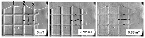 NIST MOIF (Magneto-optic imaging film) technique is unique in being able to image magnetic domains in real time while they are forming, growing and disappearing. Bright and dark regions represent stray magnetic fields as domains change. Here a series of MOIF images shows reversal of domains in a ferromagnetic film having a grid of antiferromagnetic strips on top as the external field increases to the right. Credit: Shapiro, NIST
The team was studying the behavior of nanoscale structures that sandwich thin layers of materials with differing magnetic properties. In the past few decades such structures have been the subjects of intense research because they can have unusual and valuable magnetic properties. The data read heads on modern high-density disk drives usually exploit a version of the giant magnetoresistance (GMR) effect, which uses such layered structures for extremely sensitive magnetic field detectors. Arrays of nanoscale sandwiches of a similar type might be used in future data storage devices that would outdo even today’s astonishingly capacious microdrives because in principle the structures could be made even smaller than the minimum practical size for the magnetic islands that record data on hard disk drives, according to NIST metallurgist Robert Shull.
The key trick is to cover a thin layer of a ferromagnetic material, in which the magnetic direction of electrons, or “spins,” tend to order themselves in the same direction, with an antiferromagnetic layer in which the spins tend to orient in opposite directions. By itself, the ferromagnetic layer will tend to magnetize in the direction of an externally imposed magnetic field—and just as easily magnetize in the opposite direction if the external field is reversed. For reasons that are still debated, the presence of the antiferromagnetic layer changes this. It biases the ferromagnet in one preferred direction, essentially pinning its field in that orientation. In a magnetoresistance read head, for example, this pinned layer serves as a reference direction that the sensor uses in detecting changing field directions on the disk that it is “reading.”.
Researchers have long understood this pinning effect to be a short-range phenomenon. The influence of the antiferromagnetic layer is felt only a few tens of nanometers down into the ferromagnetic layer—verticallly. But what about sideways? To find out, the NIST/ISSP team started with a thin ferromagnetic film covering a silicon wafer and then added on top a grid of antiferromagnetic strips about 10 nanometers thick and 10 micrometers wide, separated by gaps of about 100 micrometers. Using an instrument that provided real-time images of the magnetization within grid the structure, the team watched the grid structure as they increased and decreased the magnetic field surrounding it.
What they found surprised them.
As expected, the ferromagnetic material directly under the grid lines showed the pinning effect, but, quite unexpectedly, so did the uncovered material in regions between the grid lines far removed from the antiferromagnetic material. “This pinning effect extends for maybe tens of nanometers down into the ferromagnet right underneath,” explains Shull, “so you might expect that there could be some residual effect maybe tens of nanometers away from it to the sides. But you wouldn’t expect it to extend 10 micrometers away—that’s 10 thousand nanometers.” In fact, the effect extends to regions 50 micrometers away from the closest antiferromagnetic strip, at least 1,000 times further than was previously known to be possible.
The ramifications, says Shull, are that engineers planning to build dense arrays of these structures onto a chip for high-performance memory or sensor devices will find interesting new scientific issues for investigation in optimizing how closely they can be packed without interfering with each other.
* Y.P. Kabanov, V.I. Nikitenko, O.A. Tikhomirov, W.F. Egelhoff, A.J. Shapiro and R.D. Shull. Unexpectedly long-range influence on thin-film magnetization reversal of a ferromagnet by a rectangular array of FeMn pinning films. Physical Review B 79, 144435, 2009. DOI: 10.1103/PhysRevB.79.144435.