Jul 10 2009
Olympus Integrated Technologies America, Inc. (Olympus-ITA), a subsidiary of Olympus Corporation of the Americas and a leader in advanced inspection and defect review systems, announces that it has provided an infrared (IR) inspection and defect review system with metrology software to SEMATECH, the global consortium of semiconductor manufacturers, for its 3D R+D Center at the College of Nanoscale Science and Engineering's (CNSE) Albany NanoTech Complex. The system enables SEMATECH to verify alignment of bonded wafers and through silicon vias (TSV). SEMATECH's 3D program was established to deliver robust 300mm equipment and process technology solutions for high-volume TSV manufacturing.
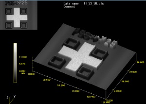
The SEMATECH 3D interconnect process using TSVs requires bonding the active side of processed wafers together. Once the wafers are bonded there is an immediate need to verify the accuracy of the bonding alignment, but the active wafer surfaces containing the alignment targets are no longer visible. The Olympus IR Inspection System allows observation and image acquisition of the alignment targets and vias by “seeing” through the 775µm thick silicon wafer to the patterned surfaces. Overlaid alignment marks are imaged and measured to verify bonding alignment accuracy. Alignment is critical for the device to function optimally. The Olympus tool was installed and accepted in April, 2009.
“Precise alignment is one of the major challenges affecting the performance of the 3D interconnects,” said Sitaram Arkalgud, SEMATECH’s director of 3D Interconnect. “Wafer bonding is a key process, and Olympus’ defect review system provides precise imaging technology that allows our researchers to address the technical challenges related to bonding interface defectivity and overlay metrology.”
“We have been collaborating with SEMATECH on inspection and defect review tools since 2001 and working with the 3D group since last year to provide a method to image and measure overlay offsets after wafers have been bonded together,” said Olympus-ITA president Greg Baker. “Olympus’ IR inspection and defect review tool with metrology functionality is now in operation at SEMATECH’s 3D R&D Center and is proving to provide very clear images and accurate measurements to help ensure via alignment and interconnectivity.”
“The SEMATECH-CNSE partnership continues to enable innovative process solutions for the manufacturing of advanced nanoscale devices,” said Richard Brilla, CNSE vice president for Strategy, Alliances and Consortia. “The addition of the Olympus IR inspection and defect review system will support that effort, while further enhancing the world-class technological capabilities of CNSE’s Albany NanoTech Complex for the benefit of our global corporate partners and the nanoelectronics industry.”
Olympus-ITA will be participating in the SEMATECH Workshop on 3D Interconnect Metrology, being held on July 15, 2009 at the San Francisco Marriott in San Francisco, CA. Richard Poplawski, on-site project manager for Olympus-ITA, will give a presentation titled 3D Interconnect Bonded Wafer Pair Metrology Using IR Microscopy. The purpose of the workshop is to gain a better understanding of how new and existing wafer metrology technologies can be utilized, modified, or enhanced to measure and improve 3D interconnect processes.