Jul 20 2009
Novelx, Inc. was just selected for a prestigious R+D 100 Award for one of the 100 most technologically significant new products in 2009. R+D Magazine recognized the Novelx mySEM® for miniaturizing and driving the cost out of the core technology inside a scanning electron microscope (SEM).
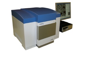
Powered by the patented Novelx Stacked Silicon Technology, the mySEM is a bench-top SEM for imaging and characterizing nanoscale objects and materials. In a compact design that installs easily into available lab space or closer to production lines, the mySEM delivers capabilities previously only available in high-end field emission SEMs, at a fraction of the cost. Optimized for low-voltage operation and without the need to coat non-conductive samples, the mySEM is an ideal choice for the imaging of energy sensitive nanomaterials, biomaterials, polymers, thin films and membranes.
Lawrence Muray, CEO and co-founder of Novelx, explains, “Novelx has designed and built a low cost, but high-performance compact field emission SEM. Our patented technology represents a disruptive innovation in how scanning electron microscopes are built and operated. By leveraging silicon processing technologies, Novelx has dramatically miniaturized the core technology inside a SEM. This miniaturization enabled the design of an all-electrostatic electron beam column that when coupled with a thermal field emission electron source is optimized for low-voltage imaging and sub-10nm resolution.”
Several imaging techniques are available with the Novelx mySEM to enhance surface contrast and allow nanoscale features to be observed. A variable low-voltage system, the mySEM eliminates charging of non-conductive samples without the need to coat samples, which can mask many nanoscale features, or to operate at increased pressure, which can degrade resolution.
According to James Spallas, CTO and co-founder of the company, “The mySEM uses a quad-segmented microchannel plate (MCP) detector. This patent-pending detector can detect secondary and backscattered electrons together, backscattered electrons only, and can operate in a topographic mode that enhances surface topography. This topographic imaging technique is capable of sub-atomic vertical resolution of crystalline materials resulting in the ability to image individual dislocations, atomic steps and other defects on or near the surface.”
Winners of the R+D 100 Awards are selected by an independent judging panel and the editors of R+D Magazine. According to Rita Peters, editorial director of R+D Magazine, “Winning an R+D 100 Award provides a mark of excellence known to industry, government, and academia as proof that the product is one of the most innovative ideas of the year.”
The Novelx mySEM is commercially available and in use by several leading university research centers for the imaging of nanoscale objects and materials in a wide variety of fields that include Materials Science and the Life Sciences. Industrial applications include the characterization of nanomaterials at corporate product development labs, the failure analysis of nanoscale defects and the quality assurance of nanomaterial-based products closer to the production line.
For additional information on the news that is the subject of this release, contact Jim Rynne or visit www.novelx.com.