The veil is being lifted from the once unseen world of molecular activity. Not so long ago only the final products were visible and scientists were forced to gauge the processes behind those products by ensemble averages of many molecules. The limitations of that approach have become clear with the advent of technologies that allow for the observation and manipulation of single molecules. A prime example is the recent first ever direct observations in real-time of the growth of single nanocrystals in solution, which revealed that much of what we thought we knew is wrong.
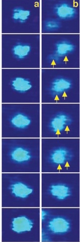 These TEM images show comparisons between the nanocrystal growth trajectories of monomer attachments (a) and coalescence events (b).
Interim Berkeley Lab Director Paul Alivisatos and Ulrich Dahmen, director of Berkeley Lab’s National Center for Electron Microscopy (NCEM), led a team of experts in nanocrystal growth and electron microscopy who combined their skills to observe the dynamic growth of colloidal platinum nanocrystals in solution with subnanometer resolution. Their results showed that while some crystals in solution grow steadily in size via classical nucleation and aggregation - meaning molecules collide and join together - others grow in fits and spurts, driven by “coalescence events,” in which small crystals randomly collide and fuse together into larger crystals. Despite their distinctly different growth trajectories, these two processes ultimately yield a nearly monodisperse distribution of nanocrystals, meaning the crystals are all approximately the same size and shape.
“Coalescence events have been previously observed in flask synthesis of colloidal nanocrystals and has been considered detrimental for achieving monodisperse colloidal nanocrystals,” says Haimei Zheng, a chemist in Alivisatos’ research group, who was the lead author on a paper that reported these results in the journal Science. “In our study, we found that coalescence events are frequently involved in the early stage of nanocrystal growth and yet monodisperse nanocrystals are still formed.”
Says Alivisatos, a chemist who holds joint appointments with Berkeley Lab and the University of California at Berkeley where he is the Larry and Diane Bock professor of Nanotechnology, “This direct observation of nanocrystal growth trajectories revealed a set of pathways more complex than those previously envisioned and enables us to re-think the nanocrystal growth mechanism with an eye towards more controlled synthesis.”
The Science paper was titled: “Observation of Single Colloidal Platinum Nanocrystal Growth Trajectories.” Co-authoring this paper with Zheng, Alivisatos and Dahmen were Rachel Smith, Young-wook Jun and Christian Kisielowski.
Nanocrystals are projected to play important roles in a wide-ranging number of technologies including solar and fuel cell, catalysis, electronics and photonics, medicine, and imaging and sensing. The key to success will be the ability to synthesis nanocrystals with desired physical properties. This will require a much better understanding of colloidal nanocrystal growth mechanisms. While the past two decades have seen tremendous advances in the synthesis of semiconductor, metal and dielectric nanocrystals, these advances have generally been realized through trial and error chemistry. A much more directed and controlled approach to nanocrystal synthesis is needed.
A new technique known as “liquid cell in situ transmission electron microscopy,” in which the powerful resolution capabilities of a transmission electron microscope (TEM) are brought to bear on a liquid cell that allows liquids to be observed inside a vacuum, enables the visualization of single nanoparticles in solution. The Berkeley researchers deployed this technique on NCEM’s JEOL 3010 In-Situ microscope. Utilizing an electron beam operating at 300 kilovolts of energy, the JEOL 3010 provides outstanding specimen penetration and spatial resolution of about 8 angstroms through the thick liquid cell sample.
“The JEOL 3010 In-Situ Microscope is our best machine for imaging dynamic events, and at 300kV the electron beam has enough penetrating power to maintain high resolution, even when looking through a liquid confined between two thin solid windows,” says NCEM director Dahmen. “Our resolution is significantly higher than any previous studies of this nature, which made it possible for us to measure the movement and growth of individual colloidal particles only a few nanometers in size.”
Zheng, Dahmen, Alivisatos and their colleagues used the JEOL 3010 and liquid cells microfabricated from a pair of 100-micron-thick silicon wafers with 20 nanometer thick silicon nitride membrane windows to image the growth trajectories of platinum nanocrystals in solution. Platinum nanocrystals are an ideal system for such studies because their high electron contrast allows liquid-cell TEM imaging of individual particles. The JEOL 3010’s electron beam was used to both trigger nucleation and drive crystal growth through reduction of the platinum cations.
“Video-rate acquisition allowed us to track nanocrystal growth trajectories from frame-to-frame,” says Zheng. “This allowed us to observe that each nanocrystal can either grow steadily through the addition of monomers from solution or by merging with another nanocrystal in random coalescence events.”
Zheng says it has been assumed that coalescence events would result in some crystals being much larger than others, a bad thing in that the physical properties of nanocrystals are so dependent upon size and shape that for many applications it is critical that monodispersed nanocrystals be produced during synthesis. Consequently, strategies such as the use of surfactants to coat nanocrystal surfaces have been adopted to avoid coalescence events.
“Our observations provide invaluable direct information on how nanocrystals grow and indicate how we might directly control nanocrystal synthesis for tailored properties,” says Zheng. “Also, our in situ liquid cell TEM technique can be applied to other areas of research such as soft matter imaging and nanoparticle catalysis, and offers great potential for addressing many fundamental issues in materials science, chemistry and other fields of science.”
Says Dahmen, “From a microscopist’s point of view, the ability to observe nanoparticles in liquid solution opens new opportunities in an area that has traditionally been off-limits because electron microscopes require vacuum conditions. We can now see directly what before could only be surmised from the statistical behavior of the ensemble. It’s like understanding traffic by watching individual cars instead of listening to the traffic report.”
NCEM is a U.S. Department of Energy national user facility that is hosted at Berkeley Lab. Established in 1983, it stands today as one of the world’s foremost centers for electron microscopy and microcharacterization.
Berkeley Lab is a U.S. Department of Energy national laboratory located in Berkeley, California. It conducts unclassified scientific research for DOE’s Office of Science and is managed by the University of California. Visit our Website at www.lbl.gov/