In a development that holds much promise for the future of solar cells made from nanocrystals, and the use of solar energy to produce clean and renewable liquid transportation fuels, researchers with the U.S. Department of Energy's Lawrence Berkeley National Laboratory (Berkeley Lab) have reported a technique by which the electrical conductivity of nanorod crystals of the semiconductor cadmium-selenide was increased 100,000 times.
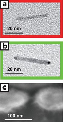 Image (a) is a transmission electron micrograph of a cadmium-selenide nanocrystal before gold tip growth in solution and image (b) is after. Image (c) is a scanning electron micrograph of a single nanocrystal two-terminal device.
“The key to our success is the fabrication of gold electrical contacts on the ends of cadmium-selenide rods via direct solution phase-growth of the gold tips,” says Paul Alivisatos, interim-Director of Berkeley Lab, who led this research. “Solution-grown contacts provide an intimate, abrupt nanocrystal-metal contact free of surfactant, which means that unlike previous techniques for adding metal contacts, ours preserves the intrinsic semiconductor character of the starting nanocrystal.”
Alivisatos is a chemist who holds joint appointments with Berkeley Lab’s Materials Sciences Division, and with the University of California-Berkeley where he is the Larry and Diane Bock professor of Nanotechnology. He is an internationally-recognized authority on nanocrystal growth and the corresponding author of a paper published in the on-line edition of Nano Letters ("Enhanced Semiconductor Nanocrystal Conductance via Solution Grown Contacts").
Co-authoring the paper with Alivisatos were Matthew Sheldon and Paul-Emile Trudeau, members of Alivisatos’ research group; Taleb Mokari, of Berkeley Lab’s Molecular Foundry; and Lin-Wang Wang, in Berkeley Lab’s Computational Research Division.
With the world demand for energy projected to more than double by 2050 and more than triple by the end of the 21st century, it is imperative that sustainable and carbon-neutral energy technologies be developed. The use of sunlight to generate electricity as well as to split water molecules for the production of fuels is envisioned as an ideal energy source, and nanocrystals could be pivotal to the success of this vision. Electrical conductance in semiconductor nanocrystals is a critical element for both solar electricity and solar fuel technologies.
“Standard contacting procedures that deposit metal onto semiconductor nanocrystals directly, such as those used in commercial wafer-scale chip fabrication, cause alloying and chemical reactions at the metal-semiconductor interface,” says Sheldon, who was the lead author on the Nano Letters paper. “This means that the finished electrical device is actually made of a different material than the starting nanocrystal.”
Sheldon notes that while chemical treatments, such as etching off surfactant, have been shown to enhance the conductivity of thin film nanocrystal solids, these treatments will often alter the semiconductor’s electrical properties, for example switching the material from n-type to p-type or altering the density of surface states. Furthermore, he says, previous studies have not explained why electrical conductance was enhanced, other than acknowledging the removal of surfactant coverage.
In this new study, Sheldon, Alivisatos and their co-authors used single nanostructure electrical measurements to make systematic comparisons between cadmium-selenide nanorods with and without gold tips. The solution-grown tipping process started with the addition of gold salt to a solution of toluene and cadmium-selenide nanorods, which resulted in gold metal being selectively deposited on the nanorod tips. A silicon wafer test chip was then dipped in this nanorod solution. After submersion, the evaporation of the toulene solvent oriented individual cadmium-selenide nanorods across pre-defined gold electrodes, which were fabricated through electron beam lithography. The results were gold-tipped cadmium-selenide heterostructure devices whose electrical conductance was characterized in a two-terminal geometry as a function of source-drain voltage and temperature.
Says Alivisatos, “Our study shows that the superior performance of gold-tipped cadmium-selenide heterostructures results from a lower Schottky barrier and that solution grown contacts do not alter the chemical composition of the semiconductor. Further, our work demonstrates the increasing sophistication of high-quality electrical devices that can be achieved through self-assembly and verifies this process as an excellent route to the next generation of electronic and optoelectronic devices utilizing colloidal nanocrystals.”
Adds Sheldon, “We believe our approach is an ideal strategy for making future devices from nanocrystals because it preserves the semiconductor character of the nanocrystal as synthesized with the precise control of their synthesis developed over the past decades.”
Sheldon says the next step in this work will be to determine if the dramatic improvements in electrical behavior can translate to improvements in nanocrystal-based energy production. Initially, the group plans to investigate the use of solution grown contacts in photovoltaic applications.