IMEC launches the industrial affiliation program (IIAP) INSITE or Integrated Solutions for Technology Exploration. INSITE is a framework of design exploration modules that allows fables and fablite companies, foundries and EDA vendors to develop design and product information using emerging IC process technologies 1 to 3 generations ahead of IC manufacturing. INSITE can be used both to design in both IMEC's emerging process technologies developed within its core CMOS research program and in more imminent foundry-level technologies targeted to early product development.
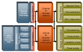 IMEC's INSITE framework of extensible, flexible modules
The INSITE program addresses two evolving trends which are creating a growing knowledge gap between the producers and users of digital CMOS technology. The first trend is the move away from integrated design and manufacturing to separate chip foundries and fables design houses. The second trend is the evolution towards more application-specific technology offerings, since technologies need to be adapted to achieve the targeted chip specification as improved speed, power, area and cost cannot be realized with the same technology.
Phillip Christie, Principal researcher at IMEC: "While the questions of fables and fab-lite companies related to designing with emerging technologies are distinct from those of foundries, EDA companies and IP vendors, the solutions to their questions require collaboration and dialog between all parties. INSITE will leverage IMEC's extensive process technology knowledge and long tradition of working at the interface between technology and design. It will provide customized solutions for the exploration of design and technology trade-offs to all players in the semiconductor value chain."
IMEC's INSITE program is set up as a modular and extensible framework that provides the required flexibility for the program partners. It comprises a design interface, circuit-level IP generation and pathfinding. The key competences of the framework are:
- An in-depth understanding of advanced process technologies and process integration;
- Fabrication and measurement of test circuits using IMEC's 200mm and 300mm wafer facilities;
- A flexible design interface to quickly couple technology advances to design flows;
- The rapid implementation of circuit-level IP;
The design interface is fully compatible and shares the same standards as design interfaces from commercial foundries. New technologies will be embedded into circuit level IP using industry-standard data formats. This ensures that products can be synthesized using emerging technologies within standard design flows in a fully transparent way. Similarly, for emerging technologies, the same library IP can be implemented as virtual libraries with limited layout information and imported into a design flow emulation environment for rapid "what if" scenario analysis.