Researchers from the National Institute of Standards and Technology (NIST) and the Naval Research Laboratory have developed a new way to introduce magnetic impurities in a semiconductor crystal by prodding it with a scanning tunneling microscope (STM). Detailed in a recent paper,* this technique will enable researchers to selectively implant atoms in a crystal one at a time to learn about its electrical and magnetic properties on the atomic scale.
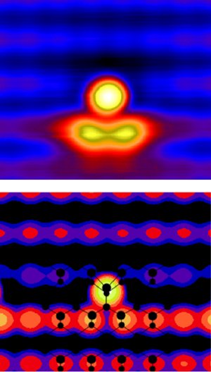 [Top] A high resolution STM image of a manganese atom (the red area, below the center) partially obscured by the large shape of a displaced indium atom in the center and two smaller arsenic atoms below. [Bottom] The theoretical model of the configuration the atoms would take when playing musical chairs. Credit: NIST
A better understanding of these properties is fundamental to the development of “spintronics,” electronic devices that will use electron spin, a characteristic of magnetism, instead of charge for storing information. Spintronics could increase the performance of electronic devices while reducing power usage and production costs.
Electronics manufacturers commonly introduce impurities into semiconducting crystals to change how well the material will conduct electricity. Researchers also can introduce impurities that induce a semiconductor to become magnetic. In these dilute magnetic semiconductors (DMS), the added impurity atoms typically must displace one of the original atoms in the crystal structure to become “active.” One of the goals of DMS materials research is to achieve higher operating temperatures by making sure all the doped magnetic impurity atoms are activated. Knowing how the impurity atoms get into the host crystal lattice sites is essential to this process.
The experiments involved depositing single manganese atoms onto an indium arsenide surface. To become active and magnetize the DMS, the manganese atom must take a chair from one of the indium atoms by occupying an indium lattice site. Using the STM probe tip, the NIST researchers zapped an indium atom with sufficient voltage to dislodge it from its place in the lattice and switch places with the manganese atom. In this way the researchers can choose where and which manganese atom they want to make active.
Because the exchange happens very quickly, researchers cannot see what path the atoms take when made to play musical chairs. To find the pathway, researchers at the Naval Research Laboratory made theoretical models of the atomic motions and identified two possible avenues for the exchange to occur. The group selected the correct pathway by comparing the calculation results with the experimental STM findings.
This work was supported in part by the Korea Research Foundation grant program (MOEHRD)**, the Office of Naval Research and the NIST-CNST/UMD-NanoCenter Cooperative Agreement. Computations were performed at the Department of Defense Major Shared Resource Center at the Air Force Research Laboratory at the Wright-Patterson Air Force Base in Ohio.
* Y.J. Song, S.C. Erwin, G.M. Rutter, P.N. First, N.B. Zhitenev and J.A. Stroscio. Making Mn substitutional impurities in InAs using a scanning tunneling microscope. Nano Letters. Published online Sept. 29, 2009. http://pubs.acs.org/doi/full/10.1021/nl902575g