At next week's SPIE Advanced Lithography Conference, to be held February 22 - 26 in San Jose, California, imec technologists contribute in a record number of over 30 papers showing their newest breakthroughs in advanced semiconductor lithography research.
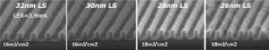 EUV resists are steadily improving and now nicely resolve 27nm LS on the EUV ADT.
While imec pushes 193nm to its limits by investigating cost-effective double patterning methods and by source mask optimization for 22nm half pitch, most research has been shifted to EUVL (extreme ultraviolet lithography). Today, EUV is the most promising cost-effective method for insertion at the 22nm node and approaches preproduction at imec by the end of 2010.
EUV approaches preproduction at imec by end 2010
With the installation of Hamatech's MaskTrack Pro photomask cleaning system, imec is now ready to start its research on EUV mask cleaning. Pristine, defect-free masks at point-of-exposure have become a critical issue in the advancement of EUVL. Since EUV masks have no protecting pellicle, each time they are handled, a risk for extra defects due to particle formation exists. As the only research facility with a complete mask integrity infrastructure, imec will now start with some of its key core partners research on innovative mask cleaning technology to make sure that EUV masks are always clean before they are loaded into the scanner. Apart from contamination by particles, potential (photon-induced) organic contamination will also be studied. This unique research will enable to develop processes of record (PORs) for EUV mask cleaning, which will allow to accelerate total process development for yielding manufacturing based on EUV lithography.
Currently, imec is developing EUV process technology by applying ASML's EUV alpha demo tool (ADT); its successor, the EUV preproduction tool (ASML NXE:3100), is scheduled for installation in Q4 2010. Using the ADT, progress has been made on many aspects of EUV Lithography and preparation for the NXE:3100 is on-going.
And promising progress has been achieved in EUV resist performance. Imec now has resists to pattern 27nm features on the alpha demo tool and is confident that suitable resists for 22nm and later on 16nm are within reach on future exposure tools. A set-up to quantify resist outgassing became operational and is now used routinely in material screening and to qualify materials for ADT exposures.
Pushing 193nm lithography towards 22nm
Imec achieved major progress in the cost reduction of double patterning. Imec compares and evaluates chemicals and techniques for litho-process-litho-etch solutions as cost effective alternatives to the litho-etch-litho-etch process. By avoiding the etch step the process cost can be reduced. First results showed a litho-process-litho-etch solution as a viable process, in the first place for designs with a repeated, regular geometry, such as memory ICs. Today, resulting from a lot of research on intelligent design split, imec also reports that litho-process-litho-etch double patterning is a suitable and cost-effective technology for random logic application at 32nm half pitch. And very good critical dimension uniformity (CDU) of the first and second patterns has been measured down to 26nm half pitch.
Imec also started a program on source mask optimization including diffractive optical elements and flexible illuminators to further push 193nm to its limits. With source mask optimization, the illumination shape is tailored to the specific layout to be printed, improving in that way the resolution and process margins to some extent.
These results show the potential to push 193nm lithography towards the 22nm node.
“I'm very proud that our lithography research team has achieved these amazing results over the last year. Thanks to their efforts and our unique infrastructure which we expand dependent on the technology needs, we are on track for cost-effective double patterning for the 32nm half pitch node and to introduce EUV at 22nm;” said Kurt Ronse, director advanced lithography program at imec.