A newly discovered path for the conversion of sunlight to electricity could brighten the future for photovoltaic technology. Researchers with Lawrence Berkeley National Laboratory (Berkeley Lab) have found a new mechanism by which the photovoltaic effect can take place in semiconductor thin-films. This new route to energy production overcomes the bandgap voltage limitation that continues to plague conventional solid-state solar cells.
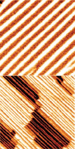 These nanoscale images of bismuth ferrite thin films show ordered arrays of 71 degree domain walls (top) and 109 degree doman walls (bottom). By changing the polarization direction of the bismuth ferrite, these domain walls give rise to the photovoltaic effect. (Image from Seidel, et. al.)
Working with bismuth ferrite, a ceramic made from bismuth, iron and oxygen that is multiferroic - meaning it simultaneously displays both ferroelectric and ferromagnetic properties - the researchers discovered that the photovoltaic effect can spontaneously arise at the nanoscale as a result of the ceramic’s rhombohedrally distorted crystal structure. Furthermore, they demonstrated that the application of an electric field makes it possible to manipulate this crystal structure and thereby control photovoltaic properties.
"We’re excited to find functionality that has not been seen before at the nanoscale in a multiferroic material," said Jan Seidel, a physicist who holds joint appointments with Berkeley Lab’s Materials Sciences Division and the UC Berkeley Physics Department. "We’re now working on transferring this concept to higher efficiency energy-research related devices."
Seidel is one of the lead authors of a paper in the journal Nature Nanotechnology that describes this work titled, "Above-bandgap voltages from ferroelectric photovoltaic devices." Co-authoring this paper with Seidel were Seung-Yeul Yang, Steven Byrnes, Padraic Shafer,Chan-Ho Yang, Marta Rossell, Pu Yu, Ying-Hao Chu, James Scott, Joel Ager, Lane Martin and Ramamoorthy Ramesh.
At the heart of conventional solid-state solar cells is a p-n junction, the interface between a semiconductor layer with an abundance of positively-charged "holes," and a layer with an abundance of negatively charged electrons. When photons from the sun are absorbed, their energy creates electron-hole pairs that can be separated within a "depletion zone," a microscopic region at the p-n junction measuring only a couple of micrometers across, then collected as electricity. For this process to take place, however, the photons have to penetrate the material to the depletion zone and their energy has to precisely match the energy of the semiconductor’s electronic bandgap - the gap between its valence and conduction energy bands where no electron states can exist.
"The maximum voltage conventional solid-state photovoltaic devices can produce is equal to the energy of their electronic bandgap," Seidel says. "Even for so called tandem-cells, in which several semiconductor p-n junctions are stacked, photovoltages are still limited because of the finite penetration depth of light into the material."
Working through Berkeley Lab’s Helios Solar Energy Research Center, Seidel and his collaborators discovered that by applying white light to bismuth ferrite, a material that is both ferroelectric and antiferromagnetic, they could generate photovoltages within submicroscopic areas between one and two nanometers across. These photovoltages were significantly higher than bismuth ferrite’s electronic bandgap.
"The bandgap energy of the bismuth ferrite is equivalent to 2.7 volts. From our measurements we know that with our mechanism we can get approximately 16 volts over a distance of 200 microns. Furthermore, this voltage is in principle linear scalable, which means that larger distances should lead to higher voltages."
Behind this new mechanism for photovoltage generation are domain walls - two-dimensional sheets that run through a multiferroic and serve as transition zones, separating regions of different ferromagnetic or ferroelectric properties. In their study, Seidel and his collaborators found that these domain walls can serve the same electron-hole separation purpose as depletion zones only with distinct advantages.
"The much smaller scale of these domain walls enables a great many of them to be stacked laterally (sideways) and still be reached by light," Seidel says. "This in turn makes it possible to increase the photovoltage values well above the electronic bandgap of the material."
The photovoltaic effect arises because at the domain walls the polarization direction of the bismuth ferrite changes, which leads to steps in the electrostatic potential. Through annealing treatments of the substrate upon which bismuth ferrite is grown, the material’s rhombohedral crystals can be induced to form domain walls that change the direction of electric field polarization by either 71, 109 or 180 degrees. Seidel and his collaborators measured the photovoltages created by the 71 and 109 degree domain walls.
"The 71 degree domain walls showed unidirectional in-plane polarization alignment and produced an aligned series of potential voltage steps," Seidel says. "Although the potential step at the 109 degree domain was higher than the 71 degree domain, it showed two variants of the in-plane polarization which ran in opposite directions."
Seidel and his colleagues were also able to use a 200 volt electric pulse to either reverse the polarity of the photovoltaic effect or turn it off altogether. Such controllability of the photovoltaic effect has never been reported in conventional photovoltaic systems, and it paves the way for new applications in nano-optics and nano-electronics.
"While we have not yet demonstrated these possible new applications and devices, we believe that our research will stimulate concepts and thoughts that are based on this new direction for the photovoltaic effect," Seidel says.
Berkeley Lab is a U.S. Department of Energy national laboratory located in Berkeley, California. It conducts unclassified scientific research and is managed by the University of California. Visit our website at http://www.lbl.gov.