Imec realized a vertical Flash transistor with Si plug diameters down to 20nm. The associated vertical Flash platform paves the way to scale Flash memory to the next nodes. The vertical device concept features enhanced performance at lower voltages as well as reduced cost.
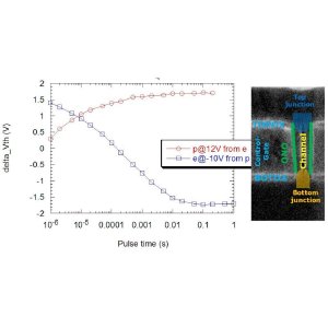 Vertical Flash transistor: Program/erase characteristics on a vertical charge trap Flash cell with poly-Si substrate and corresponding cross-section.
Floating gate Flash memory has been scaling at a tremendous pace in recent years to arrive at a startling density of 32 gigabit (4 gigabyte) on a single die today, using 30nm technology and below. Drastic device concept changes are however required for future generations to cope with the scaling limits of today’s floating gate technology. For example the electrostatic cell-to-cell interference and the low storage electron count are becoming major obstacles for further downscaling in the 20 and 10nm range.
Stacking cells in a vertical way on a chip, hence increasing the density per unit area by e.g. 8-16 for the same technology node, is a very promising approach to further push the cost down. Besides cost reduction, vertical stacking also improves the gate control and the field enhancement in the tunnel oxide because of the curvature of the gate-all-around structure. This leads to enhanced window and drive current even in the case of a poly-Si SONOS (silicon oxide nitride oxide silicon) device.
Imec designed a new process flow and all necessary test structures to optimize the vertical transistor flow. The process flow provides a gate layer and inter-gate isolation layers, which are etched all the way down to the Si (to form the so-called ‘plug’). Next, the ONO (oxide nitride oxide) memory gate stack is deposited on the sidewalls and the plug is filled with poly-Si which serves as the transistor substrate.
Plug opening, bottom junction as well as top junction profile and plug fill were found to be critical steps. Cylindrical cell structures have been obtained with Si diameters down to 20nm. A new process has been developed to allow the removal of the ONO stack at the bottom of the plug for source junction formation without damaging the tunnel oxide on the sidewalls.
Imec’s vertical Flash transistor platform will be used to investigate the scalability of this concept for the generations corresponding to the planar 1x nodes. Further experiments will include the reduction of the cell diameter, the selection of the best ONO stack taking topography into account as well as alternative channel processing schemes.
These results were obtained in collaboration with imec’s key partners in sub-22nm core CMOS research.