There’s good news in the search for the next generation of semiconductors. Researchers with the U.S. Department of Energy’s Lawrence Berkeley National Laboratory (Berkeley Lab) and the University of California (UC) Berkeley, have successfully integrated ultra-thin layers of the semiconductor indium arsenide onto a silicon substrate to create a nanoscale transistor with excellent electronic properties. A member of the III–V family of semiconductors, indium arsenide offers several advantages as an alternative to silicon including superior electron mobility and velocity, which makes it an oustanding candidate for future high-speed, low-power electronic devices.
“We’ve shown a simple route for the heterogeneous integration of indium arsenide layers down to a thickness of 10 nanometers on silicon substrates,” says Ali Javey, a faculty scientist in Berkeley Lab’s Materials Sciences Division and a professor of electrical engineering and computer science at UC Berkeley, who led this research.
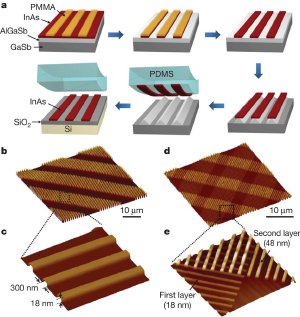 Fabricating an indium oxide (InAs) device starts with a) epitaxially growing and etching InAs into nanoribbon arrays that are get stamped onto a silicon/silica (Si/SiO2 ) substrate; b) and c) InAs nanoribbon arrays on Si/SiO2; d) and e) InAs nanoribbon superstructures on Si/SiO2.
“The devices we subsequently fabricated were shown to operate near the projected performance limits of III-V devices with minimal leakage current. Our devices also exhibited superior performance in terms of current density and transconductance as compared to silicon transistors of similar dimensions.”
For all its wondrous electronic properties, silicon has limitations that have prompted an intense search for alternative semiconductors to be used in future devices. Javey and his research group have focused on compound III–V semiconductors, which feature superb electron transport properties. The challenge has been to find a way of plugging these compound semiconductors into the well- established, low-cost processing technology used to produce today’s silicon-based devices. Given the large lattice mismatch between silicon and III-V compound semiconductors, direct hetero-epitaxial growth of III-V on silicon substrates is challenging and complex, and often results in a high volume of defects.
“We’ve demonstrated what we are calling an ‘XOI,’ or compound semiconductor-on-insulator technology platform, that is parallel to today’s ‘SOI,’ or silicon-on-insulator platform,” says Javey. “Using an epitaxial transfer method, we transferred ultrathin layers of single-crystal indium- arsenide on silicon/silica substrates, then fabricated devices using conventional processing techniques in order to characterize the XOI material and device properties.”
The results of this research have been published in the journal Nature, in a paper titled, “Ultrathin compound semiconductor on insulator layers for high-performance nanoscale transistors.” Co-authoring the report with Javey were Hyunhyub Ko, Kuniharu Takei, Rehan Kapadia, Steven Chuang, Hui Fang, Paul Leu, Kartik Ganapathi, Elena Plis, Ha Sul Kim, Szu-Ying Chen, Morten Madsen, Alexandra Ford, Yu-Lun Chueh, Sanjay Krishna and Sayeef Salahuddin.
To make their XOI platforms, Javey and his collaborators grew single-crystal indium arsenide thin films (10 to 100 nanometers thick) on a preliminary source substrate then lithographically patterned the films into ordered arrays of nanoribbons. After being removed from the source substrate through a selective wet-etching of an underlying sacrificial layer, the nanoribbon arrays were transferred to the silicon/silica substrate via a stamping process.
Javey attributed the excellent electronic performance of the XOI transistors to the small dimensions of the active “X” layer and the critical role played by quantum confinement, which served to tune the material’s band structure and transport properties. Although he and his group only used indium arsenide as their compound semiconductor, the technology should readily accommodate other compound III/V semiconductors as well.
“Future research on the scalability of our process for 8-inch and 12-inch wafer processing is needed,” Javey said.
“Moving forward we believe that the XOI substrates can be obtained through a wafer bonding process, but our technique should make it possible to fabricate both p- and n- type transistors on the same chip for complementary electronics based on optimal III–V semiconductors.
“Furthermore, this concept can be used to directly integrate high performance photodiodes, lasers, and light emitting diodes on conventional silicon substrates. Uniquely, this technique could enable us to study the basic material properties of inorganic semiconductors when the thickness is scaled down to only a few atomic layers.”
This research was funded in part by an LDRD grant from the Lawrence Berkeley National Laboratory, and by the MARCO/MSD Focus Center at MIT, the Intel Corporation and the Berkeley Sensor and Actuator Center.