May 31 2011
The new SU9000 Field Emission (FE) Scanning Electron Microscope (SEM) from Hitachi High-Technologies features novel electron optics which allow 0.4 nm resolution to be achieved at an accelerating voltage of 30 kV, with a usable magnification up to 3 Million times. This is believed to be the highest resolution-performance currently achievable on a commercially available instrument.
Featuring a new type of cold FE electron source with excellent stability and brightness and utilising Hitachi's 25 year experience of in-lens detection technology, the SU9000 also provides outstanding ultra-low current and low voltage imaging of sensitive materials. This excellent all-round performance, combined with fast specimen exchange times and the optional scanning transmission (STEM) modes, makes the SU9000 the ideal choice for use in applications ranging from semiconductor devices, electronics, and advanced nanotechnology materials, to life sciences and medicine.
The new, cold FE electron source delivers probe current that is approximately double that of earlier models, giving high quality images with superior S/N and exceptional stability from the moment the electron beam is switched on. The high performance electron optics allow a resolution of 1.2 nm at an accelerating voltage of 1 kV to be achieved without the need for beam deceleration technology. This greatly simplifies low energy imaging and significantly increases sample throughput.
Hitachi's unique dual through-the-lens detection system allows filtering of electrons of different energies, to give the capability for simultaneous multi-signal imaging. This provides extraordinary versatility for the imaging of structures and surface properties.
Using the scanning transmission (STEM) option, the SU9000 guarantees STEM resolution that can allow the lattice structure of graphite (C (002) d=0.34 nm) to be imaged at 30 kV accelerating voltage. The unique STEM detection system allows simultaneous bright field and dark field imaging and annular DF detection with selectable scattering angle. Up to 4 signals can be simultaneously displayed.
The SU9000 features side-entry sample insertion and can be ready for high resolution imaging in as little as 6 minutes or less; the fast exchange times benefiting from the high stability of the electron beam.
An order of magnitude better vacuum around the sample minimizes contamination, enhancing resolution and eliminating the need for an additional cold trap for cryo work on biological samples.
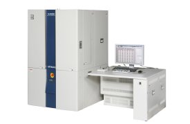
Ease of use is guaranteed through a new user interface, while a large 24.1-inch widescreen monitor offers a comfortable environment for both operating the instrument and viewing images.