A significant milestone in extreme ultraviolet (EUV) lithography was reported by Cymer's David Brandt last week at SPIE Advanced Lithography 2013 in San Jose. The event, which drew more than 2200 attendees, ran Feb. 24-28.
“There was much discussion about the continuation of Moore’s law, both in terms of the technical ability to shrink as well as the cost,” said symposium chairman Harry J. Levinson of Globalfoundries Inc. “Achievement of a significant milestone for EUV sources that should enable more rapid progress in EUV lithography was reported, as was the potential for a EUV pellicle — a welcomed prospect. And EUV extension to higher resolution, where we face many challenges, was the subject of many papers.”
Cymer Inc. announced Thursday that it had met “key milestones” in recent tests of its EUV technology in an ASML Holding NV lithography scanner.
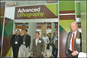 The energy on the exhibition floor at the opening of SPIE Advanced Lithography 2013 reflected the energy in the conference rooms: a very positive sense of real progress toward delivery beyond research in new technical alternatives including directed self-assembly and EUV. Courtesy of SPIE.
The energy on the exhibition floor at the opening of SPIE Advanced Lithography 2013 reflected the energy in the conference rooms: a very positive sense of real progress toward delivery beyond research in new technical alternatives including directed self-assembly and EUV. Courtesy of SPIE.
David Brandt, Cymer’s senior director of EUV marketing, reported new results for EUV power output as a light source for lithography, including a key announcement of 40 W of EUV light in continuous operation using master oscillator power amplifier (MOPA) prepulse technology.
“In addition to the good news of EUV source power achievements, there were first signs of considerations for EUV adoption in high volume, coming from infrastructure development such as EUV mask actinic inspection, EUV mask OPC [optical proximity correction], and EUV lithography integration in a full CMOS flow with yield-defectivity investigations,” said symposium co-chairman Mircea Dusa of ASML US.
Directed self-assembly (DSA) was also a subject of high interest at the conference, Dusa said. “What caught my attention was the modeling developments combined with applicability on real circuits — a major milestone for future potential adoption.”
Levinson and Dusa also noted the event’s high level of topical synergy, evidenced by multiple joint sessions on topics such as lithographic solutions for chip-design layout, and its characteristic large conference-room audiences, particularly in the Etch and Metrology, and Process Control conferences.
“Developers and executives in the chip-making industry tell us that SPIE Advanced Lithography continues to be the must-attend meeting,” said Peter Hallett, SPIE director of marketing and industry relations. “This is where significant technology achievements are announced, where R&D challenges are discussed up and down the supply chain, and where lithographic tools and techniques are introduced.”
A well-trafficked two-day exhibition connected attendees with semiconductor suppliers, integrators and optical device manufacturers, and professional development courses on EUV lithography, DSA, optical lithography and related technologies began the week.
Accepted conference proceedings papers will be published in the SPIE Digital Library upon approval and also will appear in print volumes and digital collections.
Advanced Lithography 2014 will be held Feb. 23-27 in San Jose.