Researchers from the National Institute of Standards and Technology (NIST) and the University of Maryland have shown how to make nanoscale measurements of critical properties of plasmonic nanomaterials—the specially engineered nanostructures that modify the interaction of light and matter for a variety of applications, including sensors, cloaking (invisibility), photovoltaics and therapeutics.
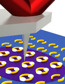 Infrared laser light (purple) from below a sample (blue) excites ring shaped nanoscale plasmonic resonator structures (gold). Hot spots (white) form in the rings' gaps. In these hot spots, infrared absorption is enhanced, allowing for more sensitive chemical recognition. A scanning AFM tip detects the expansion of the underlying material in response to absorption of infrared light. Credit:NIST
Their technique is one of the few that allows researchers to make actual physical measurements of these materials at the nanoscale without affecting the nanomaterial's function.
Plasmonic nanomaterials contain specially engineered conducting nanoscale structures that can enhance the interaction between light and an adjacent material, and the shape and size of such nanostructures can be adjusted to tune these interactions. Theoretical calculations are frequently used to understand and predict the optical properties of plasmonic nanomaterials, but few experimental techniques are available to study them in detail. Researchers need to be able to measure the optical properties of individual structures and how each interacts with surrounding materials directly in a way that doesn't affect how the structure functions.
"We want to maximize the sensitivity of these resonator arrays and study their properties," says lead researcher Andrea Centrone. "In order to do that, we needed an experimental technique that we could use to verify theory and to understand the influence of nanofabrication defects that are typically found in real samples. Our technique has the advantage of being extremely sensitive spatially and chemically, and the results are straightforward to interpret."
The research team turned to photothermal induced resonance (PTIR), an emerging chemically specific materials analysis technique, and showed it can be used to image the response of plasmonic nanomaterials excited by infrared (IR) light with nanometer-scale resolution.
The team used PTIR to image the absorbed energy in ring-shaped plasmonic resonators. The nanoscale resonators focus the incoming IR light within the rings' gaps to create "hot spots" where the light absorption is enhanced, which makes for more sensitive chemical identification. For the first time, the researchers precisely quantified the absorption in the hot spots and showed that for the samples under investigation, it is approximately 30 times greater than areas away from the resonators.
The researchers also showed that plasmonic materials can be used to increase the sensitivity of IR and PTIR spectroscopy for chemical analysis by enhancing the local light intensity, and thereby, the spectroscopic signal.
Their work further demonstrated the versatility of PTIR as a measurement tool that allows simultaneous measurement of a nanomaterial's shape, size, and chemical composition—the three characteristics that determine a nanomaterial's properties. Unlike many other methods for probing materials at the nanoscale, PTIR doesn't interfere with the material under investigation; it doesn't require the researcher to have prior knowledge about the material's optical properties or geometry; and it returns data that is more easily interpretable than other techniques that require separating the response of the sample from response of the probe.
For background on PTIR, see the February 2013 NIST Tech Beat story, "NIST Captures Chemical Composition with Nanoscale Resolution" at www.nist.gov/public_affairs/tech-beat/tb20130220.cfm#ptir.
Source: http://www.nist.gov/