Researchers at the Department of Energy’s Oak Ridge National Laboratory and the University of Tennessee, Knoxville have pioneered a new technique for forming a two-dimensional, single-atom sheet of two different materials with a seamless boundary.
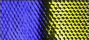 ORNL and UT researchers have invented a method to merge different 2-dimensional materials into a seamless layer. This colorized scanning tunneling microscope image shows a single-atom sheet composed of graphene (seen in blue) combined with hexagonal boron nitride (seen in yellow). Credit: ORNL
The study, published in the journal Science, could enable the use of new types of 2-D hybrid materials in technological applications and fundamental research.
By rethinking a traditional method of growing materials, the researchers combined two compounds -- graphene and boron nitride -- into a single layer only one atom thick. Graphene, which consists of carbon atoms arranged in hexagonal, honeycomb-like rings, has attracted waves of attention because of its high strength and electronic properties.
“People call graphene a wonder material that could revolutionize the landscape of nanotechnology and electronics,” ORNL’s An-Ping Li said. “Indeed, graphene has a lot of potential, but it has limits. To make use of graphene in applications or devices, we need to integrate graphene with other materials.”
One method to combine differing materials into heterostructures is epitaxy, in which one material is grown on top of another such that both have the same crystalline structure. To grow the 2-D materials, the ORNL-UT research team directed the growth process horizontally instead of vertically.
The researchers first grew graphene on a copper foil, etched the graphene to create clean edges, and then grew boron nitride through chemical vapor deposition. Instead of conforming to the structure of the copper base layer as in conventional epitaxy, the boron nitride atoms took on the crystallography of the graphene.
“The graphene piece acted as a seed for the epitaxial growth in two-dimensional space, so that the crystallography of the boron nitride is solely determined by the graphene,” UT’s Gong Gu said.
Not only did the team’s technique combine the two materials, it also produced an atomically sharp boundary, a one-dimensional interface, between the two materials. The ability to carefully control this interface, or “heterojunction,” is important from an applied and fundamental perspective, says Gu.
“If we want to harness graphene in an application, we have to make use of the interface properties, since as Nobel laureate Herbert Kroemer once said ‘the interface is the device,’” Li said. “By creating this clean, coherent, 1-D interface, our technique provides us with the opportunity to fabricate graphene-based devices for real applications.”
The new technique also allows researchers to experimentally investigate the scientifically intriguing graphene-boron nitride boundary for the first time.
“There is a vast body of theoretical literature predicting wonderful physical properties of this peculiar boundary, in absence of any experimental validation so far,” said Li, who leads an ORNL effort to study atomic-level structure-transport relationships using the lab’s unique four-probe scanning tunneling microscopy facility. “Now we have a platform to explore these properties.”
The research team anticipates that its method can be applied to other combinations of 2-D materials, assuming that the different crystalline structures are similar enough to match one another.
The study is titled “Heteroepitaxial Growth of Two-Dimensional Hexagonal Boron Nitride Templated by Graphene Edges.”
Coauthors are the University of Tennessee’s Gong Gu, Lei Liu, and Wan Deng; ORNL’s Jewook Park, Kendal Clark, Juan Carlos Idrobo, Leonardo Basile and An-Ping Li; and Sandia National Laboratories’ David Siegel and Kevin McCarty.
This work was partially supported by the National Science Foundation, the Defense Advanced Research Projects Agency, and the National Secretariat of Higher Education, Science, Technology and Innovation of Ecuador. Work at Sandia was supported by DOE’s Office of Science.
Part of this research was conducted at the Center for Nanophase Materials Sciences, which is sponsored at ORNL by the Scientific User Facilities Division in DOE’s Office of Basic Energy Sciences. CNMS is one of the five DOE Nanoscale Science Research Centers supported by the DOE Office of Science, premier national user facilities for interdisciplinary research at the nanoscale. Together the NSRCs comprise a suite of complementary facilities that provide researchers with state-of-the-art capabilities to fabricate, process, characterize and model nanoscale materials, and constitute the largest infrastructure investment of the National Nanotechnology Initiative. The NSRCs are located at DOE's Argonne, Brookhaven, Lawrence Berkeley, Oak Ridge and Sandia and Los Alamos national laboratories. For more information about the DOE NSRCs, please visit http://science.energy.gov/bes/suf/user-facilities/nanoscale-science-research-centers/.
ORNL is managed by UT-Battelle for the Department of Energy's Office of Science. DOE's Office of Science is the single largest supporter of basic research in the physical sciences in the United States, and is working to address some of the most pressing challenges of our time. For more information, please visit http://science.energy.gov.
Source: http://www.ornl.gov/