Faster electronic device architectures are in the offing with the unveiling of the world's first fully two-dimensional field-effect transistor (FET) by researchers with the Lawrence Berkeley National Laboratory (Berkeley Lab). Unlike conventional FETs made from silicon, these 2D FETs suffer no performance drop-off under high voltages and provide high electron mobility, even when scaled to a monolayer in thickness.
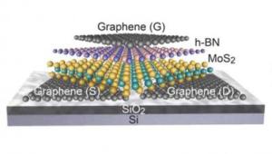 Berkeley Lab researchers fabricated the first fully 2-D field-effect transistor from layers of molybdenum disulfide, hexagonal boron nitride and graphene held together by van der Waals bonding. Credit: Image courtesy of Ali Javey, Berkeley Lab
Ali Javey, a faculty scientist in Berkeley Lab's Materials Sciences Division and a UC Berkeley professor of electrical engineering and computer science, led this research in which 2D heterostructures were fabricated from layers of a transition metal dichalcogenide, hexagonal boron nitride and graphene stacked via van der Waals interactions.
"Our work represents an important stepping stone towards the realization of a new class of electronic devices in which interfaces based on van der Waals interactions rather than covalent bonding provide an unprecedented degree of control in material engineering and device exploration," Javey says. "The results demonstrate the promise of using an all-layered material system for future electronic applications."
Javey is the corresponding author of a paper describing this research in ACS Nano titled "Field-Effect Transistors Built from All Two-Dimensional Material Components". Co-authors are Tania Roy, Mahmut Tosun, Jeong Seuk Kang, Angada Sachid, Sujay Desai, Mark Hettick and Chenming Hu.
FETs, so-called because an electrical signal sent through one electrode creates an electrical current throughout the device, are one of the pillars of the electronics industry, ubiquitous to computers, cell phones, tablets, pads and virtually every other widely used electronic device. All FETs are comprised of gate, source and drain electrodes connected by a channel through which a charge-carrier - either electrons or holes – flow. Mismatches between the crystal structure and atomic lattices of these individual components result in rough surfaces – often with dangling chemical bonds - that degrade charge-carrier mobility, especially at high electrical fields.
"In constructing our 2D FETs so that each component is made from layered materials with van der Waals interfaces, we provide a unique device structure in which the thickness of each component is well-defined without any surface roughness, not even at the atomic level," Javey says. "The van der Waals bonding of the interfaces and the use of a multi-step transfer process present a platform for making complex devices based on crystalline layers without the constraints of lattice parameters that often limit the growth and performance of conventional heterojunction materials."
Javey and his team fabricated their 2D FETs using the transition metal dichalcogenide molybdenum disulfide as the electron-carrying channel, hexagonal boron nitride as the gate insulator, and graphene as the source, drain and gate electrodes. All of these constituent materials are single crystals held together by van der Waals bonding.
For the 2D FETs produced in this study, mechanical exfoliation was used to create the layered components. In the future, Javey and his team will look into growing these heterogeneous layers directly on a substrate. They will also look to scale down the thickness of individual components to a monolayer and the lengths of the channels to molecular-scale dimensions.
Source: http://www.lbl.gov/