At Ferdinand-Braun-Institute (FBH) in Berlin LayTec's EpiCurve®TT HR (High Resolution) sensor is successfully used to optimise the external quantum efficiency and the emission wavelength of LEDs for near UV spectral region. Dr. Arne Knauer and co-workers apply the sensor for monitoring of composition of AlGaN and InAlGaN barrier layers.
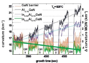 Wafer curvature during growth of different InAlGaN barriers at 825°C between identical InGaN quantum wells.
Since the Indium incorporation is highly sensitive to the temperature, small changes of the surface temperature caused e.g. by the wafer bow during growth can result in large variations of the In content in the InAlGaN layers. The team at FBH grew multiple quantum well (MQW) structures with GaN, Al- GaN and InAlGaN barriers with different In content (between 0% and 5%) and compared the wafer curvature of the calibration layers and of the multiple quantum well (MQW) barrier layers. Fig. 2 shows the development of the curvature signal during the deposition of barrier layers with different compositions stemming from different growth runs.
The growth of nearly unstrained GaN and of In0.03Al0.16Ga0.81N barriers (red curve) results in a nearly constant curvature. The In0.05Al0.16Ga0.79N barriers (green curve) grow under compression and therefore the curvature signal decreases. The Al0.16Ga0.84N barriers (black curve) are under tensile stress and the curvature increases. This data demonstrates the possibility to monitor not only stress, but also the composition of extremely thin layers (8 nm).
The results of the study have been submitted for publication in Physica status solidi, Proceedings of the 3rd International Symposium on Semiconductor Light Emitting Devices (ISSLED) Phoenix, USA, April 27-May 2, 2008. For further information please contact [email protected].