At Semicon Korea 2009, SUSS MicroTec (FWB:SMH)(GER:SMH) unveiled the second generation of its ACS300, a modular system for coating, baking and developing of wafers up to 300mm. The ACS300 Gen2 offers unmatched configuration flexibility at market-leading cost of ownership.
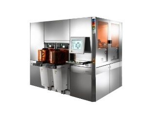 Frontview ACS300 Gen2 modular coat/bake/develop system from SUSS MicroTec (Photo: Business Wire)
The system architecture and process modules are specifically adapted to the needs of the advanced packaging and 3D integration industry, which requires very thick photo resist layers of up to 100 microns and more. Combining best in class coat and develop uniformity with exceptional edge bead performance makes the ACS300 Gen2 the preferred solution for various special spin coating applications such photosensitive polymers like polyimide, PBO or Cyclotene™ (BCB).
The ACS300 Gen2 continues the success of the preceding model, ACS300Plus with developments driving equipment cost down, extending overall equipment efficiency and scaling down of the footprint.
"Addressing the specific requirements for wafer level packaging and 3D integration the new ACS300 is equipped with various packaging specific features, which makes it specifically suited for applications like solder bumping, gold bumping or redistribution layers," said Rolf Wolf, General Manager of SUSS MicroTec Lithography Division. "The next generation ACS300 will definitively help SUSS MicroTec to continue and further expand its market leading position in the field of advanced packaging, and extending it into 3D processing."
Posted January 20th. 2009