JPK Instruments, a world-leading manufacturer of nanoanalytic instrumentation for research in life sciences and soft matter, is pleased to announce a new accessory for its NanoWizard® product line.
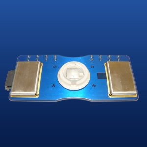 JPK's new Conductive AFM module for the NanoWizard AFM family
The new conductive AFM module for JPK's NanoWizard® II AFM maps local conductivity changes. Operating in contact, intermittent contact and spectroscopy modes, applications include charge mapping in polymers, organic semiconductors, nanotubes and nanoparticles.
Conductive AFM (CAFM), records the current flowing between an electrically conductive cantilever (typically Pt/Ir or Cr/Pt) and substrate while a bias is applied between tip and sample. JPK's new conductive AFM accessory attaches directly to the base of the NanoWizard head. An ultra-sensitive pre-amplifier enables detection of sub picoamp currents. Bias voltage is software selected with range +/- 10 Volts. Conductivity mapping can be carried out in both contact and intermittent contact modes, under ambient or oxygen-free conditions, whilst simultaneously displaying the surface topography image. Powerful spectroscopy software allows the variation in current to be tracked as the potential is ramped at user defined locations. This is referred to as current voltage (I/V) spectroscopy.
The sample holder supplied with the NanoWizard® II CAFM module supports metal stubs, glass slides and cover slips. A separate holder is used for optically transparent samples enabling simultaneous measurement of fluorescence. A spring loaded electrode guides the bias voltage to the sample surface. Alternatively, conductive lacquer can be used. Samples can also be prepared on HOPG and other electrically conductive flat samples such as indium tin oxide (ITO). Applications include metals, semiconductors, polymers, ferroelectrics, dielectrics and organic conductors.