Jul 6 2009
X-rays can be used to image hidden structures such as bones of the human body. But now, a team of Würzburg physicists has succeeded in demonstrating the electronic structure of an interface in a solid for the first time.
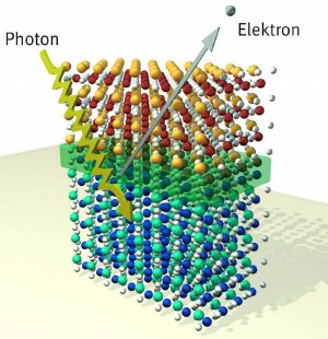 Solids of two oxide materials at whose interface an electron gas has formed (green area). The expansion and density of electron gas has been precisely determined for the first time by physicists from the University of Würzburg. This has been achieved by using x-ray-induced photoemission spectroscopy (explanation in the text). Figure: Götz Berner.
Why should such interfaces be researched? "They are important for the functioning of electronic components such as transistors," says Michael Sing from the Department for Experimental Physics IV at the University of Würzburg. Anyone who wants to improve or develop such components should therefore know the properties of interfaces very well.
A very special interface has been analyzed by the Würzburg physicists in collaboration with members from the University of Augsburg and the Paul Scherrer Institut in Switzerland: They covered a carrier substrate of strontium titanate with some very thin layers of lanthanum aluminate. They were interested in the region where the two materials converge.
Why exactly these materials? Although both materials are good insulators, they do conduct current if brought together. "At the boundary between them, a conducting layer is formed, a so-called electron gas that becomes superconducting at very low temperatures and will then carry a current without loss," Michael Sing explains. In addition, the conductivity of the layer can be turned on and off. That is why these materials are very attractive for future applications.
Electron gas: Measuring density and thickness
Although the conducting layer between the materials has been detected in 2004, it is now that a team of scientists has determined its thickness and density with high precision for the first time. Thickness and density are significant parameters of the electronic properties of conducting layers.
Result: The conducting electrons are only present in a single layer of the strontium titanate, directly at the inner boundary layer to the aluminate. "As the electrically conducting layer is so thin - it only consists of one atomic layer - this structure might be used in the future to further lessen the sizes of components such as computer chips," Michael Sing says.
Prospect: Components for aggressive environments
Both materials might be suitable to act as an alternative to silicon which is the most important base material in present semiconductor industry. According to the Würzburg scientists, silicon-based components show the following disadvantages: They do not work properly in temperatures above 200 degrees Celsius or below the freezing point.
It is different with so-called oxide ceramics, a material group to which lanthanum aluminate and strontium titanate belong. According to Michael Sing, oxide ceramics are suitable for use in aggressive environments, for example in incineration plants or aerospace applications - places with very high or very low temperatures.
Next target: Analyzing a working component
The next goal the Würzburg physicists want to achieve is to analyze the electrically conducting interface in a working component. In order to do so, they want to use a field-effect transistor on the basis of lanthanum aluminate and strontium titanate. From the experiments, they want to gain more knowledge about what happens in such a layer structure during current switching operations.
Measurement method
The researchers describe their experiments in the Physical Review Letters. They used a modern variant of the so-called x-ray-induced photoemission spectroscopy. The method is based on the well-established photo effect: Electrons absorb x-rays; thus, they absorb a lot of energy and they are accelerated. Their high speed enables them now to penetrate several atomic layers in a solid and escape the material through its surface.
This is where the fast electrons are detected and their speed is measured. And this allows drawing conclusions about what type of atom they come from and about the current charge state of the atoms. "If the irradiated x-ray energy is varied, and with it the extent to which the electrons leave the solid, it is possible to produce an electronic and chemical depth profile and reconstruct from it an image of the inspected structure," Michael Sing explains.
Profiling the interface electron gas of LaAlO3/SrTiO3 heterostructures by hard X-ray photoelectron spectroscopy, M. Sing, G. Berner, K. Goß, A. Müller, A. Ruff, A. Wetscherek, S. Thiel, J. Mannhart, S.A. Pauli, C.W. Schneider, P.R. Willmott, M. Gorgoi, F. Schäfers und R. Claessen, Physical Review Letters 102, 176805 (2009), doi 10.1103/PhysRevLett.102.176805