Scientists at the U.S. Department of Energy's (DOE) Brookhaven National Laboratory, in collaboration with researchers from Hitachi High Technologies Corp., have demonstrated a new scanning electron microscope capable of selectively imaging single atoms on the top surface of a specimen while a second, simultaneous imaging signal shows atoms throughout the sample's depth. This new tool, located at Brookhaven Lab's Center for Functional Nanomaterials (CFN), will greatly expand scientists' ability to understand and ultimately control chemical reactions, such as those of catalysts in energy-conversion devices.
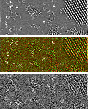 Uranium single atoms (circled) and small crystallites on a carbon support imaged simultaneously using a scanning probe to produce forward scattering through the sample (top) and backward scattering emerging from the surface (bottom). Center panel shows superimposition of the two in red (bulk) and green (surface). Atoms not seen in the lower image are on the bottom surface of the support.
A paper describing the work will be published online September 20, 2009, in Nature Materials, along with a commentary article highlighting the development.
“Our knowledge of the role of individual atoms in nanotechnology and energy-related research is strongly influenced by our ability to visualize them, not only in bulk but also on the surface, which is where the interactions of chemical reactions take place,” said Brookhaven physicist Yimei Zhu, lead author on the paper. “This new microscope and the method we developed allow us, for the first time, to directly look at atoms on the top surface and in the bulk of a sample simultaneously to reveal their atomic arrangement and bonding states. This information will help us identify the active sites and functions of materials at nanoscale dimensions for a wide range of applications, such as converting waste heat or chemical energy to electricity.”
Like all scanning electron microscopes, the new tool probes a sample with an electron beam focused to a tiny spot and detects so-called secondary electrons emitted by the sample to reveal its surface structure and topography. Though this technique has been a workhorse of surface imaging in industrial and academic laboratories for decades, its resolution has left much to be desired because of imperfect focusing due to lens aberrations.
Using a newly developed spherical aberration corrector, the new tool corrects these distortions to create a smaller probe with significantly increased brightness.
“The effect is similar to using a larger aperture lens on a camera,” said biophysicst Joseph Wall, a longtime expert in electron microscopy at Brookhaven Lab and a co-author on the paper. “It allows you to gather information from a larger angle and focus on a smaller spot.”
The new device also employs specialized electron optics to channel the emitted secondary electrons to the detector. The result is a fourfold improvement in resolution to below one tenth of a nanometer — and thus, the ability to image single atoms.
Additional detectors, located below the sample, detect electrons transmitted through the sample, revealing details about the entire structure at the exact instant the “shutter” snapped to record each pixel of the surface image. This simultaneous imaging allows the scientists to correlate information in the two images to understand precisely what is happening on the surface and throughout the sample at the same time.
“Having information about the surface structure and the bulk sample at the same time will allow researchers to better determine how the surface and bulk atoms work together, for example in a catalytic reaction,” said Zhu. The improved resolution and combined imaging capabilities will also reveal features such as small variations in composition or the locations of impurities that could have large effects on function.
“An essential component of this study was selection of a test specimen, isolated uranium atoms on a thin carbon substrate, where the images could be interpreted quantitatively to rule out other possible interpretations,” Wall commented.
Because of its extreme sensitivity, the new microscope must be kept isolated from a range of environmental effects such as variations in temperature, mechanical vibrations, and electromagnetic fields. Even the slightest waft of air could cause distortions in the images.
Fortunately the CFN was built with these needs in mind. Temperatures are regulated to within three-hundredths of a degree Fahrenheit over a 24-hour period; shock-absorber-like slabs isolate the room from the rumble of passing trucks and distant slamming doors; layers of heavy doors keep even subtle vibrations out; and air-cooling panels replace typical ceiling vents to eliminate airflow.
“The building is really a mechanical-engineering masterpiece,” said Zhu. “This microscope wouldn't work at all without these sophisticated systems.” Development of the microscope was funded by the Office of Basic Energy Sciences within the DOE Office of Science.