Imec sets major step towards 20nm half pitch interconnects with the realization of electrically functional copper lines embedded into silicon oxide using a spacer-defined double patterning approach.
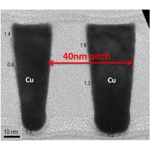 Cross sectional TEM analysis of 20nm ½ pitch interconnects after integration into single damascene using a spacer defined double patterning approach.
“We are very proud to be the world’s first in developing and processing such small on-pitch working interconnects;” said Zsolt Tokei, program director interconnects at imec. “Spacer-defined (or self-aligned) double patterning has recently gained interest as the patterning technique for future FLASH memory devices. I’m confident that memory companies will benefit from this state-of-the-art result.”
Scaling of interconnects towards 20nm half pitch faces many challenges. Double patterning lithography is needed since the metal lines cannot be realized in a single print. Therefore, a solution is needed for the actual design split of the structures and the alignment of the different masks. And, filling of (sub-)20nm lines is not possible using standard physical vapor deposition of TaN/Ta-based metallization. Moreover, control of line-edge roughness becomes increasingly difficult with further scaling. And finally, engineering of the patterning stack is required for optimal adhesion.
Imec demonstrated patterning and metallization of 20nm half pitch copper lines in silicon oxide with a TiN metal hard mask. The patterning is based on a sacrificial double hard mask and uses 3 photos (CORE, TRIM and PATCH) and four etch steps. The CORE photo defines dense lines at 40nm half pitch, which after trim, etch and spacer deposition results in 20nm half pitch spacer loops. The TRIM makes large openings to cut the spacer loops away by etch. And PATCH defines the final layout, electrical connections and bond pads. Overlay control is critical in order to end up with the designed test pattern. The dielectric spacing between the metal lines was accurately controlled thanks to the spacer-defined integration method. A Ruthenium-based metallization scheme was used to realize void-less filling.
Dielectric breakdown properties of the interconnects were measured and the results are very encouraging as the breakdown field is close to the intrinsic dielectric breakdown properties of the oxide and dielectric cap layers.
These results were obtained in cooperation with imec’s key partners in its core CMOS programs: Intel, Micron, Panasonic, Samsung, TSMC, Sony, Fujitsu, Infineon, Qualcomm, ST Microelectronic, Amkor.
Imec performs world-leading research in nanoelectronics. Imec leverages its scientific knowledge with the innovative power of its global partnerships in ICT, healthcare and energy. Imec delivers industry-relevant technology solutions. In a unique high-tech environment, its international top talent is committed to providing the building blocks for a better life in a sustainable society. Imec is headquartered in Leuven, Belgium, and has offices in Belgium, the Netherlands, Taiwan, US, China and Japan. Its staff of more than 1,750 people includes over 550 industrial residents and guest researchers. In 2009, imec's revenue (P&L) was 275 million euro.
Imec is a registered trademark for the activities of IMEC International (a legal entity set up under Belgian law as a "stichting van openbaar nut”), imec Belgium (IMEC vzw supported by the Flemish Government), imec the Netherlands (Stichting IMEC Nederland, part of Holst Centre which is supported by the Dutch Government), imec Taiwan (IMEC Taiwan Co.) and imec China (IMEC Microelectronics (Shangai) Co. Ltd.).