In typical plasmonic devices, electromagnetic waves crowd into tiny metal structures, concentrating energy into nanoscale dimensions.
Due to coupling of electronics and photonics in these metal nanostructures, plasmonic devices could be harnessed for high-speed data transmission or ultrafast detector arrays. However, studying plasmonic fields in nanoscale devices presents a real roadblock for scientists, as examining these structures inherently alters their behavior.
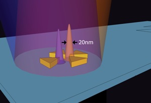 By imaging fluorescence from gold within a bowtie-shaped plasmonic device, Berkeley Lab researchers gleaned the position of plasmonic modes just a few nanometers apart.
“Whether you use a laser or a light bulb, the wavelength of light is still too large to study plasmonic fields in nanostructures. What’s more, most tools used to study plasmonic fields will alter the field distribution—the very behavior we hope to understand,” says Jim Schuck, a staff scientist with Lawrence Berkeley National Laboratory (Berkeley Lab) who works in the Imaging and Manipulation of Nanostructures Facility at the Molecular Foundry.
Light microscopy plays a fundamental role in a scientist’s repertoire: the technique is easy to use and doesn’t inflict damage to a carefully crafted electronic circuit or delicate biological specimen. However, a typical nanoscale object of interest—such as a strand of DNA or a quantum dot—is well below the wavelength of visible light in size, which means the ability to distinguish one such object from another when they are closely spaced is lost. Scientists are now challenging this limit using ‘localization’ techniques, which count the number of photons emanating from an object to help determine its position.
In previous work, Schuck and colleagues at the Molecular Foundry, a U.S. Department of Energy (DOE) Nanoscale Science Research Centers, engineered bowtie-shaped plasmonic devices designed to capture, filter and steer light at the nanoscale. These nano-color sorter devices served as antennae to focus and sort light in tiny spaces to a desired set of colors or energies—crucial for filters and other detectors.
In this latest advance, Schuck and his Berkeley Lab team used their innovative imaging concept to visualize plasmonic fields from these devices with nanoscale resolution. By imaging fluorescence from gold within the bowtie and maximizing the number of photons collected from their bowtie devices, the team was able to glean the position of plasmonic modes—oscillations of charge that result in optical resonance—just a few nanometers apart.
“We wondered whether there was a way to use light already present in our bowties—localized photons—to probe these fields and serve as a reporter,” says Schuck. “Our technique is also sensitive to imperfections in the system, such as tiny structural flaws or size effects, suggesting we could use this technique to measure the performance of plasmonic devices in both research and development settings.”
In parallel with Schuck’s experimental findings, Jeff Neaton, Director of the Molecular Foundry ’s Theory of Nanostructured Materials Facility and Alex McLeod, an undergraduate student working at the Foundry, developed a web-based toolkit, designed to calculate images of plasmonic devices with open-source software developed at Massachusetts Institute of Technology. For this study, the researchers simulated adjusting the structure of a double bowtie antenna by a few nanometers to study how changing the size and symmetry of a plasmonic antenna affects its optical properties.
“By shifting their structure by just a few nanometers, we can focus light at different positions inside the bowtie with remarkable certainty and predictability,” said McLeod. “This work demonstrates that these nanoscale optical antennae resonate with light just as our simulations predict.”
Useful for researchers studying plasmonic and photonic structures, this toolkit will be available for download on nanoHUB, a computational resource for nanoscience and technology created through the National Science Foundation’s Network for Computational Nanotechnology.
“This work really exemplifies the very best of what the Molecular Foundry is about,” said Neaton, who is also Acting Deputy Director of Berkeley Lab’s Materials Sciences Division. “Three separate Foundry facilities—Imaging, Nanofabrication and Theory—collaborated on a significant advance in our understanding of how visible light can be localized, manipulated, and imaged at the nanoscale.”
A paper reporting this research titled, “Non-perturbative visualization of nanoscale plasmonic field distributions via photon localization microscopy,” appears in Physical Review Letters and is available to subscribers online. Co-authoring the paper with Schuck, McLeod and Neaton were Alexander Weber-Bargioni, Zhaoyu Zhang, Scott Dhuey, Bruce Harteneck and Stefano Cabrini.
Portions of this work at the Molecular Foundry were supported by DOE’s Office of Science. Support for this work was also provided by the National Science Foundation through the Network for Computational Nanotechnology.
The Molecular Foundry is one of the five DOE Nanoscale Science Research Centers (NSRCs), national user facilities for interdisciplinary research at the nanoscale, supported by the DOE Office of Science. Together the NSRCs comprise a suite of complementary facilities that provide researchers with state-of-the-art capabilities to fabricate, process, characterize and model nanoscale materials, and constitute the largest infrastructure investment of the National Nanotechnology Initiative. The NSRCs are located at DOE’s Argonne, Brookhaven, Lawrence Berkeley, Oak Ridge and Sandia and Los Alamos National Laboratories.
Source: http://www.lbl.gov/