CEA-Leti today announced the companies have entered into a three year agreement to characterize advanced semiconductor materials for the 22nm technology node and beyond. European-based CEA-Leti, with its two partners on the NanoCharacterization Platform of MINATEC Campus, CEA-Liten (new materials for new energies) and CEA-INAC (Nanoscience Institute), will apply their expertise in holography and nanobeam diffraction.
FEI will provide advanced nanobeam diffraction technology with its Titan scanning transmission electron microscope (S/TEM), the world's most powerful, commercially-available microscope. The companies will measure strain changes in semiconductor structures.
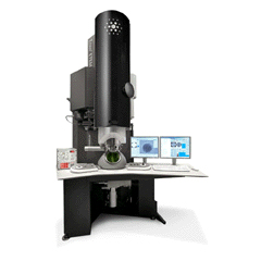 The FEI Titam TEM
"The research will focus on two important areas: use of holography with the Titan's unique XFEG electron source to improve the sensitivity of dopant profiling, and the use of nanobeam diffraction techniques to measure changes in strain and other crystallographic parameters," said George Scholes, vice president and general manager for FEI's S/TEM product line. "With the Titan, FEI is a leader in these areas and we look forward to partnering with CEA-Leti on their unique platform for characterization and nanoscale in continuing to advance the technology."
"We must improve the sensitivity, accuracy and throughput of dopant profiling in order to continue supporting shrinking device dimensions. And a better understanding of the effects of strain is critical in the development of higher performance IC devices as we continue to push the technology to the 22nm technology node and beyond," stated Rudy Kellner, vice president and general manager of FEI's Electronics Division.
According to Laurent Malier, CEO of CEA-Leti, "We chose to work with FEI on this three year research project, not only because of their powerful, commercially-available microscope, but also because of their special expertise in nanobeam diffraction applications. Together, we expect to address several critical technical roadblocks facing the semiconductor industry as it continues to push the device size and performance envelope and also challenges in the characterization of materials used in nanoelectronics and more generally for nanosciences."