Applied Materials has established its presence in defect inspection scanning electron microscope (SEM) technology with the introduction of the first-of-its-kind tool called the Applied SEMVision G5 system that allows chip manufacturers to image and study 20 nm yield-limiting imperfections with no manual interference.
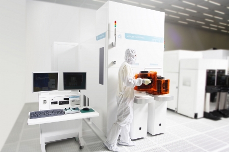 Applied SEMVision G5 system
The SEMVision G5 system can image and detect imperfections down to 1 nm pixel size. With the system, memory and logic customers can now streamline their production and detect the cause of imperfections precisely and rapidly. With its unprecedented image quality, advanced 1 nm pixel size and potent inspection engine, the DR-SEM system detects and examines imperfections in the intricate patterning layers, while improving output.
The SEMVision G5 system sets unique standards differentiating real and false alarms or in detecting nuisance defects. Its accuracy and operation speed are far better than a skilled operator, making customers quickly examine more number of wafers, which in turn improves yield ramp rates and cycles of learning.
Open architecture platform, the SEMVision G5 system allows the merging of information obtained from a wafer inspection device with a collection of predefined inspection strategies. The system eliminates the need to create strategies manually, as it can generate inspection strategies automatically, based on the type of chips to be examined. This feature helps foundry companies to achieve rapid production of their range of chip designs with high output.
Applied Materials’ Corporate Vice President and General Manager for Process Diagnostics and Control business unit, Itai Rosenfeld stated that with its hands-free approach and superior imaging functionalities, the SEMVision G5 system helps customers decrease market-reach time, which is important to attain the short product cycles.
Source: http://www.appliedmaterials.com