A research team led by Nader Engheta from the University of Pennsylvania is working on ways to use light in place of electricity. The team has developed the first physical illustration of ‘lumped’ optical circuit elements using nanotechnology.
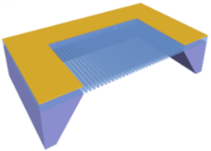 An illustration of an array of silicon nitrite nanorods. The entire array is about half a millimeter long.
The physical demonstration is a landmark in an emerging field of science and engineering, called as ‘metatronics’ by Engheta. The research findings have been reported in Nature Materials.
In the experiment, the research team built a comb-like structure comprising arrays of silicon nitrite nanorods. The word ‘meta’ in ‘metatronics’ denotes metamaterials, an emerging research field where nanostructures and patterns are embedded in materials so that they can manipulate waves in unprecedented ways.
In the study, the gaps between the nanorods and their cross-sections create a pattern that imitates the functions of capacitors, inductors and resistors, the three fundamental circuit components, but in optical wavelengths. The research team used an optical signal with a mid-infrared range wavelength for illuminating the nanorods. The team then measured the wave when it passed via the comb-like structure using spectroscopy. It then repeated the procedure on nanorods having nine different dimensions. What it discovered was the change in optical current and optical voltage caused by the optical capacitors, inductors and resistors with parameters in line with those variations in size.
Engheta explained that the air gap functions as a capacitor, while a cross-section of the nanorod functions as both a resistor and inductor. Beyond altering the nanorods’ base material and their dimensions, these optical circuits’ function can also be changed by altering the light’s orientation, enabling metatronic circuits to access patterns that are not possible in conventional electronics.
Changing the orientation of light in metatronics is analogous to rewiring an electric circuit. Engheta called a metatronic circuit as ‘stereo-circuitry’ because the orientation delivers two different circuits. Based on its success with fundamental optical components, the research team plans to use the principle to build complex three-dimensional structures using nanorod arrays because an optical signal knocking such a structure’s top may meet a different circuit when compared to a one knocking its side. The team is now focusing on designing more complex optical components, Engheta concluded.