A research team led by Professors Gabriel Popescu and Lynford Goddard from the University of Illinois has developed an inexpensive technique using a special kind of microscope to etch delicate features on the surface of semiconductors, while simultaneously monitoring the entire process in real time with nanoscale resolution.
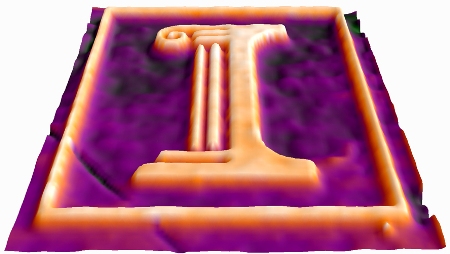 This is a three-dimensional image of the University of Illinois logo etched into a gallium-arsenide semiconductor, taken during etching with a new microscopy technique that monitors the etching process on the nanometer scale. The height difference between the orange and purple regions is approximately 250 nanometers. (photo by Chris Edwards, Amir Arbabi, Gabriel Popescu, and Lynford Goddard)
The microscope utilizes two light beams to image and carve the topography with very high precision. Goddard informed that the concept is based on the possibility of measuring the structure’s height when the light gets reflected off from different surfaces. The etch rate can be determined by observing the changes in height, enabling the team to monitor the etching process. This, in turn, enables the team to determine the etch rate across space as well as across time at every spot on the semiconductor wafer that comes within the field of view of the microscope.
Existing techniques of scanning tunneling microscopy or atomic force microscopy are not capable of monitoring the etching process in its progress. The new technique is faster, less noisy, inexpensive, and is purely optical, which enables the monitoring of the entire wafer at once rather than point-by-point without touching the semiconductor surface.
Besides observing the etching process, the light acts as a catalyst for the process dubbed photochemical etching. To create required features, masks with unique patterns of gray are used to shine the light by degrees, a process which is time consuming and expensive. By comparison, in the new technique, a grayscale image is shined onto the sample under etching using a projector, thus allowing the team to form intricate patterns easily and rapidly, as well as adjust them whenever required by simply changing the projector pattern.
According to the researchers, this method shows promise in real-time monitoring of the self assembly of carbon nanotubes or in error monitoring in large-scale production of computer chips. It may facilitate chipmakers to lower processing time and expenses by continuously ensuring the calibration of their equipment.
Source: http://www.illinois.edu