Dec 14 2012
On the road to smaller, high-performance electronics, University of Illinois researchers have smoothed one speed bump by shrinking a key, yet notoriously large element of integrated circuits.
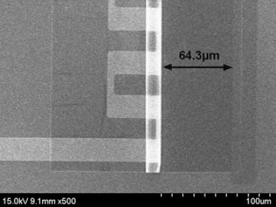
 These are experimental images of a self-rolled inductor, printed on a very thin film of silicon nitrate. (Credit: Xiuling LI)
Three-dimensional rolled-up inductors have a footprint more than 100 times smaller without sacrificing performance. The researchers published their new design paradigm in the journal Nano Letters.
"It's a new concept for old technology," said team leader Xiuling Li, a professor of electrical and computer engineering at the University of Illinois.
Inductors, often seen as the sprawling metal spirals on computer chips, are essential components of integrated circuits. They store magnetic energy, acting as a buffer against changes in current and modulating frequency – especially important in radio-frequency wireless devices. However, they take up a lot of space. Inductance depends on the number of coils in the spiral, so engineers cannot make them smaller without losing performance.
In addition, the larger the area the inductor occupies, the more it interfaces with the substrate the chip is built on, exacerbating a hindering effect called parasitic capacitance. Researchers have developed some three-dimensional inductor structures to solve the dual problems of space and parasitic capacitance, but these methods are complex and use techniques that are difficult to scale up to manufacturing levels.
The new inductor design uses techniques Li's group previously developed for making thin films of silicon nitrate, merely tens of nanometers in thickness, that roll themselves up into tubes. The research team used industry-standard two-dimensional processing to pattern metal lines on the film before rolling, creating a spiral inductor.
"We're making 3-D structures with 2-D processing," Li said. "Instead of spreading this out in a large area to increase inductance, we can have the same inductance but packed into a much smaller area."
Using the self-rolling technique, the researchers can shrink the area needed for a radio-frequency inductor to a scant 45 microns by 16 microns – more than 100 times smaller than the area an equivalent flat spiral would require.
The design can be adjusted to fit target parameters including metal thickness and type, frequency, tube diameter and number of turns. According to Li, this technique could be used for capacitors and other integrated circuit elements as well.
Now, Li's group is working to produce high-performance inductor prototypes, in collaboration with electrical and engineering professor Jose Schutt-Aine. Preliminary experimental data show strong correlation with the modeled designs.
"Once we have optimized this process, we should be able to make an integrated circuit with a completely different platform that could be much smaller," Li said. "It's an ambitious goal."
Source: http://www.uiuc.edu