Mar 29 2013
The union of theory and practice makes broadband, low-loss optical devices practical, which is why two groups of Penn State engineers collaborated to design optical metamaterials that have custom applications that are easily manufactured.
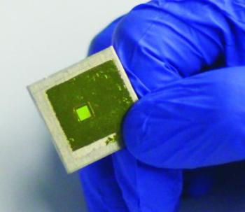 A photograph of the fabricated free-standing metamaterial filter thin-film mounted on an optical frame. Credit: Penn State
Metamaterials are manufactured materials that derive their unusual properties from structure rather than only composition, and possess exotic properties not usually found in nature. Nanostructured metamaterials appear different for signals of different frequencies. They are dispersive, so that if researchers manipulate this material dispersion, they gain a comprehensive control of the device performance across a band of frequencies.
In the past, to control the optics of metamaterials, researchers used complicated structures including 3-dimensional rings and spirals that are difficult if not impossible to manufacture in large numbers and small sizes at optical wavelengths. From a practical perspective, simple and manufacturable nanostructures are necessary for creating high-performance devices.
"We must design (nanostructures that can be fabricated," said Theresa S. Mayer, Distinguished Professor of Electrical Engineering and co-director of Penn State's nanofabrication laboratory.
Designing materials that can allow a range of wavelengths to pass through while blocking other wavelengths is far more difficult than simply creating something that will transmit a single frequency. Minimizing the time domain distortion of the signal over a range of wavelengths is necessary, and the material also must be low loss.
"We don't want the signal to change as it passes through the device," said Jeremy A. Bossard, postdoctoral fellow in electrical engineering.
The majority of what goes in must come out with little absorption or distortions to the signal waveform due to the metamaterial dispersion.
"What we do is use global optimization approaches to target, over wide bandwidths, the optical performance and nano fabrication constraints required by different design problems," said Douglas H. Werner, John L. and Genevieve H. McCain Chair Professor of Electrical Engineering. "The design methodology coupled with the fabrication approach is critically important."
The design team looked at existing fishnet structured metamaterials and applied nature-inspired optimization techniques based on genetic algorithms. They optimized the dimensions of features such as the size of the fishnet and the thicknesses of the materials. One of the transformative innovations made by the researchers was the inclusion of nanonotches in the corners of the fishnet holes, creating a pattern that could be tuned to shape the dispersion over large bandwidths. They reported their approach in today's (Mar. 28) online issue of Scientific Reports.
"We introduced nanonotches in the corners of the air holes to give a lot more flexibility to independently control the properties of permittivity and permeability across a broad band," said Werner. "The conventional fishnet doesn't have much flexibility, but is easy to fabricate."
Permittivity measures the ease or difficulty of inducing an electric field in a material, while permeability measures the ease or difficulty of inducing a magnetic field. Theoretically, manipulating permittivity and permeability allows tuning of the metamaterial across a range of wavelengths and creates the desired index of refraction and impedance.
Theory may provide a solution, but can that solution become reality? The fabrication team placed constraints on the design to ensure that the material could be manufactured using electron-beam lithography and reactive ion etching. The initial material was a three-layer sandwich of gold, polyimide and gold on oxidized silicon. When the silicon dioxide mask and the electron beam resist are removed, the researchers were left with an optical metamaterial with the desired properties.
In this case they created a band pass filter, but the same principles can be applied to many optical devices used in optical communications systems, medicine, testing and characterization or even optical beam scanning if the metamaterial is shaped to form a prism.
Another use of this metamaterial could be in conjunction with natural materials that do not have the desired properties for a specific optical application.
"All materials have a natural dispersion," said Mayer. "We might want to coat a natural material in some regions to compensate for the dispersion."
According to Werner, currently the only way to compensate is to find another natural material that would do the job. Only rarely does such a material exist.
Source: http://www.psu.edu/