Apr 23 2013
Recent progress in the engineering of plasmonic structures has enabled new kinds of nanometer-scale optoelectronic devices as well as high-resolution optical sensing. But until now, there has been a lack of tools for measuring nanometer-scale behavior in plasmonic structures which are needed to understand device performance and to confirm theoretical models.
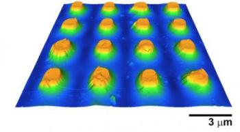 This is an atomic force microscope image of plasmonic semiconductor microparticles. Credit: William P. King, University of Illinois at Urbana-Champaign
"For the first time, we have measured nanometer-scale infrared absorption in semiconductor plasmonic microparticles using a technique that combines atomic force microscopy with infrared spectroscopy," explained William P. King, an Abel Bliss Professor in the Department of Mechanical Science and Engineering (MechSE) at Illinois. "Atomic force microscope infrared spectroscopy allows us to directly observe the plasmonic behavior within microparticle infrared antennas."
The article describing the research, "Near-field infrared absorption of plasmonic semiconductor microparticles studied using atomic force microscope infrared spectroscopy," appears in Applied Physics Letters.
"Highly doped semiconductors can serve as wavelength flexible plasmonic metals in the infrared," noted Daniel M. Wasserman, assistant professor of electrical and computer engineering at Illinois. "However, without the ability to visualize the optical response in the vicinity of the plasmonic particles, we can only infer the near-field behavior of the structures from their far-field response. What this work gives us is a clear window into the optical behavior of this new class of materials on a length scale much smaller than the wavelength of light."
The article compares near-field and far-field measurements with electromagnetic simulations to confirm the presence of localized plasmonic resonance. The article further reports high resolution maps of the spatial distribution of absorption within single plasmonic structures and variation across plasmonic arrays.
"The ability to measure near field behavior in plasmonic structures allows us to begin expanding our design parameters for plasmonic materials," commented Jonathan Felts, a MechSE graduate student. "Now that we can measure the optical behavior of individual features, we can start to think about designing and testing more complex optical materials."
Source: http://engineering.illinois.edu/