Jun 24 2014
ZEISS introduces the next generation of photomask qualification system AIMS™ 1x-193i at this year´s European Mask and Lithography Conference (EMLC) in Dresden. ZEISS has experience in aerial imaging technology and AIMS™ for more than 20 years and has become a defacto-industry standard for printability analysis of mask defects.
The new system supports the further extension of 193nm lithography and meets the challenging requirements of advanced lithography techniques such as Multi-Patterning and Source Mask Optimization.
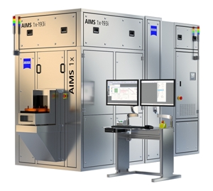 The new AIMS 1x-193i convinces with a completely redesigned optical system and increased throupghput. (Photo: Business Wire)
AIMS™ enables the user to qualify the optical performance of a mask under scanner equivalent illumination conditions. The AIMS™ 1x-193i works with 193nm illumination and benefits from a completely redesigned optical system. By utilizing FlexIllu® it provides the highest level of illumination flexibility as it is able to read the scanner files for illumination. FlexIllu® sets the scanner illumination settings computer controlled.
Thanks to the advances in the optical design as well as major improvements in the software the AIMS™ 1x-193i achieves significantly reduced turnaround-times. The enhanced pupil uniformity realizes best scanner and tool-to-tool matching.
Another highlight is a significantly improved CD repeatability enabling more accurate defect qualification that stays ahead of the requirements of the ITRS roadmap as the industry move to smaller feature sizes.
“The total number as well as the complexity of masks increases with every node due to Multi-Patterning techniques and complex mask designs. AIMS™ 1x-193 matches the tight requirements of high-end mask makers in terms of accuracy, efficiency and cycle time,” states Ute Buttgereit, Senior Product Manager AIMS™.
The first tool has achieved excellent results during customer acceptance procedure and was shipped to their facility. To maintain the high performance and productivity demanded by leading-edge customers, the AIMS™ 1x-193i systems are supported by ZEISS´ global comprehensive service network.
Semiconductor Manufacturing Technology
The Semiconductor Manufacturing Technology business group includes the Lithography Optics, Laser Optics and Semiconductor Metrology Systems business units. With a broad portfolio of products and globally leading know-how in the areas of lithography and optical modules, the business group covers various key processes in microchip production: as a developer and manufacturer of lithography optics, for example, the Lithography Optics business unit is a technology and market leader in this sector of the semiconductor industry. The portfolio of Laser Optics includes optical components for lithography lasers and subsystems for wafer inspection systems. With its inspection, repair and metrology systems, Semiconductor Metrology Systems focuses on the photomask, one of the core components of chip fabrication. In fiscal year 2011/12 the business group generated revenue of around 967 million euros with a workforce of about 2,600 people. The business group is headquartered in Oberkochen, Germany.
Source: http://www.zeiss.com