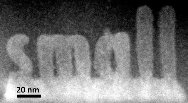
 A structure sculpted by the researchers using their novel technique
The new technique, which uses scanning transmission electron microscopy (STEM) can be used to build 3D structures with atomic precision. The technique is already showing use in understanding the quantum and electronic behavior of nanosized materials and is hoped to be used in the manufacturing of nanochips
The research, carried out at Oak Ridge National Laboratory and led by Albina Borisevich, showed how scanning electron microscopes could be used to precisely sculpt 3D nanoscale structures from complex oxides. Conventionally scanning transmission electron microscopes (STEMs) are only used to observe nanoscale structures and not to create them.
The use of a STEM allows structures to be constructed with atomic scale precision, meaning the technique could be used to accurately produce microchips. The structures display epitaxial growth, meaning they grow with a perfectly crystalline alignment.
This high degree of order is difficult to achieve using conventional methods and ensures that all of the material exhibits the same electrical and mechanical properties.
We can make smaller things with more precise shapes. The process is also epitaxial, which gives us much more pronounced control over properties than we could accomplish with other approaches.
Albina Borisevich - ORNL
As with lots of scientific breakthroughs the method was discovered serendipitously; the team were actually trying to correctly image an imperfect strontium titanate thin film. The film, which consisted of an amorphous layer of strontium titinate overlaid on a crystalline layer of the same compound, changed shape as the electron beam was transmitted through it.
When we exposed the amorphous layer to an electron beam, we seemed to nudge it toward adopting its preferred crystalline state. It does that exactly where the electron beam is.
Albina Borisevich - ORNL
Using a STEM, which transmits a beam of electrons through the substrate to be sculpted, deviates from conventional sculpting methods such as lithography that work by manipulating or patterning a materials surface.
We're using fine control of the beam to build something inside the solid itself. We're making transformations that are buried deep within the structure. It would be like tunneling inside a mountain to build a house.
Stephen Jesse - ONRL
The STEM technique occurs via a 'knock-on-process' where the electron beam transfers energy to the sample, as opposed to heating an area of it.
"With the electron beam, we are injecting energy into the system and nudging where it would otherwise go by itself, given enough time. Thermodynamically it wants to be crystalline, but this process takes a long time at room temperature.
Albina Borisevich - ORNL
The new method will also increase the efficiency of some materials research. Many researchers in the field of nanotechnology are interested in how a materials characteristics can change with it's thickness.
This relationship is extremely important on the nanoscale, where the laws of quantum mechanics govern, and a materials electronic behavior is highly thickness dependent.
Until now, researchers have had to take measurements of many individual samples, each of a slightly different thickness, to determine this. However, using the new STEM technique individual atomic layers could be added to the sample, one at a time, with measurements taken in-between each laters addition.
The whole premise of nanoscience is that sometimes when you shrink a material it exhibits properties that are very different than the bulk material. Here we can control that. If we know there is a certain dependence on size, we can determine exactly where we want to be on that curve and go there.
Albina Borisevich - ORNL
The research has been published as "Atomic-level sculpting of crystalline oxides: towards bulk nanofabrication with single atomic plane precision."