Jan 22 2016
With an investment of more than 500 000 euros, the new facilities will allow the manufacture of all kinds and forms of graphene as well as the development of electronic nanodevices for IoT (Internet of Things) applications, biosensors, and 'wereable' devices attached to the clothes
The University of Granada (UGR) has launched the Graphene and Bi-dimensional Semiconductors Laboratory, one of the most complete public laboratories devoted to the manufacture and electric and structural characterization of this material in Europe. This laboratory is comparable to that of the University of Cambridge (United Kingdom) or the one in the University of Stanford (United States).
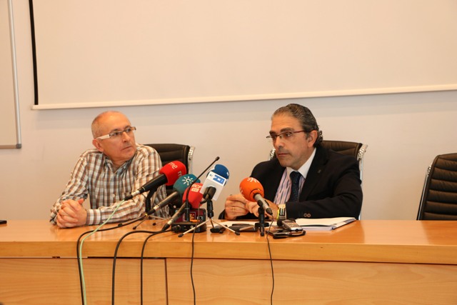
The new facilities, managed by the Group of Nanoelectronics lead by professor Francisco Gámiz Pérez, are located in the UGR Research Centre for Information Technology and Communication (CITIC-UGR, from its abbreviation in Spanish). They have been presented to the public this morning in a press conference attended by Enrique Herrera Viedma, vice dean of Research and Transfer.
With an investment of more than half a million euros, the new laboratory is devoted to the manufacture of all kinds and forms of graphene as well as the development of new graphene-based systems for electronic applications which include biosensors, electronic nanodevices for IoT (Internet of Things) applications, and flexible electronics, in addition to 'wereable' devices (those which are attached to clothes and always on).
When, in 2004, researchers Andrei Geim and Kostya Novoselov from the University of Manchester obtained a graphene sheet using adhesive tape a piece of graphite similar to that of the pencil leads, they were far from imagining the impact that such a simple action would have in the scientific community and in our lives over the next years.
Graphene is a very thin sheet comprised of a single layer of carbon atoms with spectacular mechanical, optical and electrical properties. It's a transparent, flexible and very hard material with really high electrical and thermal conductivity. All of those properties make graphene potentially usable in a lot of cases. It has such a great potential that the European Commission has made graphene one of its flagship projects for the next years, with an investment of more than 500 million euros until 2023.
Different kinds of graphene
The CITIC-UGR new Nanoelectronics Laboratory has installed the necessary equipment for obtaining CVD graphene sheets of a size up to 25 cm x 10 cm and transferring them to different substrates (rigid and flexible substrates alike).
This equipment completes the laboratory of electrical and nano-structural characterization already available in the CITIC. The materials developed can be electrically and structurally characterized in the UGR facilities (thanks to the equipment purchased, which includes an atomic-force microscope) and functionalized for its use as biosensors.
Along with CVD (Chemical Vapour Deposition) graphene, they have also developed the methods for obtaining graphene oxide suspensions from graphite dust. Graphene oxide suspension can be deposited on different substrates for reducing it later, thus obtaining reduced graphene (rGO) using a kind of dip-pen lithography system.
"This method allows us to obtain graphene patterns and graphene bi-dimensional structures on different substrates with which to develop flexible antennas and sensors, and RF-tags (tiny devices similar to stickers that can be adhered to a product, animal or person and that have an antenna to receive and respond to radio-frequency requests", Francisco Gámiz, director of the UGR Graphene Laboratory, explains.
Not only graphene
Apart from graphene, the new facilities allow to obtain other bi-dimensional materials that, combined with graphene, improve and widen its field of action.
These bi-dimensional materials, known as transition metals dichalcogenides (TMDs), such as molybdenum disulfide, molybdenum selenide or tungsten selenide, can be 'stacked' for forming structures with which to develop nanoelectronic devices and, from them, developing systems in the field of flexible electronics, such as the above mentioned 'wereables'.
Source: http://canalugr.es/