Mar 16 2016
U.S. government nanotechnology researchers have developed a new approach to understand the nanoworld operations, which are medically and technologically important processes that occur between solids and liquids, such as along cell membranes or in batteries.
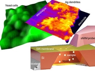 NIST and ORNL scientists have devised a near-field microwave imaging approach to capture images of nanoscale processes under natural conditions. As the tip of an atomic force microscope scans over an ultrathin membrane it emits near-field microwaves into the sample below. Shown are images of yeast cells and silver dendrites that formed on an electrode during electroplating. (Credit: Kolmakov/CNST)
The new approach is a microwave imaging technique, which is better than electron-based and X-ray methods that can cause damage to delicate samples and spoil the results. It avoids exposing expensive equipment to liquids, and eliminates the need to harden probes against toxic, corrosive, or other harsh environments.
The new approach was described by the collaborators from the Center for Nanoscale Science and Technology at the National Institute of Standards and Technology (NIST) and the Department of Energy’s (DOE) Oak Ridge National Laboratory (ORNL), in the journal ACS Nano. The approach can be used to image biological and reactive samples at nanoscales under realistic conditions.
The important element is a window, which is a thin membrane separating the needle-like probe in an atomic force microscope (AFM) from the sample that is held in minute containers with a consistent gas or liquid environment. The addition modifies near-field microwave imaging into a comprehensive tool, expanding its use to cover the field of gases and liquids. In semiconductor technology, the tool is utilized to examine solid structures.
The ultrathin, microwave-transparent membrane allows the sample to be examined in much the same way that Earth’s radar was used to reveal images of the surface of Venus through its opaque atmosphere. We generate microwaves at the apex—or very end—of the probe tip. The microwaves penetrate through the membrane a few hundred nanometers deep into the liquid up to the object of interest. As the tip scans the sample from across the membrane, we record the reflected microwaves to generate the image.
Andrei Kolmakov, Physicist, NIST
Microwaves are larger than nanoscale objects, though the waves are used to “see” the objects. However when the microwaves are emitted from only a small distance away, they are reflected from a sample, and produce a surprisingly detailed image.
The NIST-ORNL team, for their proof-of-concept experiments, employed a hybrid microscope to acheive a nanoscale view of the initial stages of a silver electroplating process. Microwave images provided the electrochemical formation of dendrites or branching metal clusters on electrodes. Features measuring nearly 100 nm (billionths of a meter) could be discerned.
The microwaves were too weak to cut chemical bonds, heat up, or interfere in any other way with the image capturing process. Conversely, a scanning electron microscope, which when utilized to record the same electroplating process at comparable resolution levels, produced images that displayed delamination and other damaging effects to the electron beam.
The NIST-ORNL group reported identical success when using its AFM-microwave set-up in order to record photographs of yeast cells that were dispersed in glycerol or water. Spatial resolution levels matched those realized with a scanning electron microscope, and as mentioned earlier, the images were devoid of any damage caused by the electron beam.
In their experiments, the group utilized a membrane made up of silicon dioxide or silicon nitride with thickness of 8 to 50 nm. The researchers found that better resolution, down to tens of nanometers, and a larger probing depth of up to hundreds of nanometers can be obtained with thinner membrane.
These numbers can be improved further with tuning and development of better electronics.
Andrei Kolmakov, Physicist, NIST
Other than examining processes in toxic, reactive, or radioactive environments, the scientists feel that the new microwave-imaging technique can be integrated into “lab-on-a-chip” fluidic devices for sampling gases and liquids.
The research was conducted at NIST’s Center for Nanoscale Science and Technology and at the Center for Nanophase Materials Sciences, a DOE Office of Science User Facility.