Jul 19 2016
In a recent work published in Nature Communications, the research group led by ICREA Professor at ICFO Frank Koppens demonstrate a novel way to detect low-energy photons using vertical heterostructures made by stacking graphene and other 2D semiconducting materials. By studying the photoresponse of these atomically thin sandwiches, the researchers have shown that it is possible to generate a current by heating electrons in graphene with infrared light and extracting the hottest electrons over a vertical energy barrier.
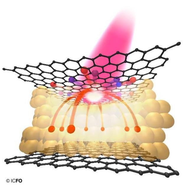 Artistic view of the photo-thermionic effect in a graphene-WSe2-graphene heterostructure. (CREDIT: ©ICFO| Fabien Vialla)
This ingenious mechanism, named photo-thermionic effect, takes advantage of the unique optical properties of graphene such as its broadband absorption, ultrafast response and gate-tunability. Moreover, owing to their vertical geometry, devices relying on this effect make use of the entire surface of graphene and can be potentially scaled up and integrated with flexible or rigid platforms.
More generally, this study reveals once again the amazing properties of these man-made heterostructures. According to Prof. Frank Koppens \"this is just the tip of the iceberg, these 2D sandwiches still have a lot to reveal”. ICFO researcher Mathieu Massicotte, first author of this study, emphasizes the new possibilities opened up by these new materials: “Everyone knows it is possible to detect light with graphene using in-plane geometries, but what about the out-of-plane direction? To answer, you need to think outside the 2D box!”
The results obtained from this study have shown that heterostructures made of 2D materials and graphene can be used to detect low-energy photons which could lead to new, fast and efficient optoelectronic applications, such as high-speed integrated communication systems and infrared energy harvesting. In addition, it demonstrates the compatibility of 2D materials with the digital chips currently utilized in cameras, paving the way for low cost infrared spectrometers and imaging systems.
Source: https://www.icfo.eu/