Oct 6 2016
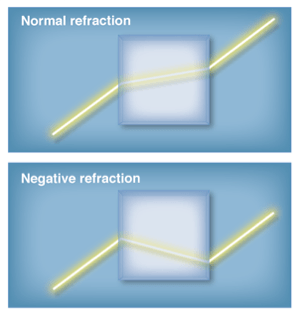 An illustration of refraction through a normal optical medium versus what it would look like for a medium capable of negative refraction. (Photo courtesy of Cory Dean)
Negative refraction for electrons traveling across a boundary between two regions in a conducting material has been discovered by a team of researchers.
The team was headed by Cory Dean, assistant professor of physics at Columbia University, Avik Ghosh, professor of electrical and computer engineering at the University of Virginia, and James Hone, Wang Fong-Jen Professor of Mechanical Engineering at Columbia Engineering.
This effect was initially predicted in 2007 and has been hard to validate experimentally. The team was able to observe the effect in graphene, illustrating that electrons in the atomically thin material act in the same manner as light rays, which can be controlled by optical devices like prisms and lenses.
The findings of the research are published in the September 30 edition of Science, and are likely to pave the way for the development of new types of electron switches, built on the theories of optics instead of electronics.
The ability to manipulate electrons in a conducting material like light rays opens up entirely new ways of thinking about electronics. For example, the switches that make up computer chips operate by turning the entire device on or off, and this consumes significant power. Using lensing to steer an electron ‘beam’ between electrodes could be dramatically more efficient, solving one of the critical bottlenecks to achieving faster and more energy efficient electronics. These findings could also enable new experimental probes. For example, electron lensing could enable on-chip versions of an electron microscope, with the ability to perform atomic scale imaging and diagnostics. Other components inspired by optics, such as beam splitters and interferometers, could additionally enable new studies of the quantum nature of electrons in the solid state.
Cory Dean, Assistant Professor, Columbia University
Graphene has been investigated extensively to support high electron speed, however it is very hard to turn off the electrons without hurting their mobility. Ghosh says, “The natural follow-up is to see if we can achieve a strong current turn-off in graphene with multiple angled junctions. If that works to our satisfaction, we’ll have on our hands a low-power, ultra-high-speed switching device for both analog (RF) and digital (CMOS) electronics, potentially mitigating many of the challenges we face with the high energy cost and thermal budget of present day electronics.”
The direction of light changes - or refracts - when traveling from one material to another, a process that enables the use of prisms and lenses to focus and guide light. A quantity known as the index of refraction establishes the degree of bending at the boundary, and is positive for traditional materials such as glass.
However, through smart engineering, it is also achievable to develop optical “metamaterials” with a negative index, where the angle of refraction is also negative.
This can have unusual and dramatic consequences. Optical metamaterials are enabling exotic and important new technologies such as super lenses, which can focus beyond the diffraction limit, and optical cloaks, which make objects invisible by bending light around them.
James Hone, Columbia Engineering
Electrons passing through highly pure conductors can pass in straight lines similar to light rays, enabling optics-like phenomena to come through. In materials, the role of electron density is similar to that of the index of refraction, and electrons refract when they travel from a region of one density to another.
Current carriers in materials can either act like they are positively charged (holes) or negatively charged (electrons), based on whether they dwell in the valence or conduction band. In reality, boundaries between electron-type or hole-type conductors, known as p-n junctions (“p” positive and “n” negative), form the building blocks of electrical devices such as transistors and diodes.
“Unlike in optical materials”, says Hone, “where creating a negative index metamaterial is a significant engineering challenge, negative electron refraction occurs naturally in solid state materials at any p-n junction.”
In the 1980s and 1990s the creation of 2D conducting layers in high-purity semiconductors such as gallium arsenide (GaAs) enabled scientists to showcase electron optics including the effects of both lensing and refraction. However, in these materials, electrons pass without dispersing only at very low temperatures, restricting technological applications.
The occurrence of an energy gap between the valence and conduction band disperses electrons at interfaces and prevents observation of negative refraction in semiconductor p-n junctions. In this research, the team’s application of graphene, a 2D material with unmatched performance at room temperature without any energy gap overcame both of these restrictions.
In 2007, the prospect of negative refraction at graphene p-n junctions was first put forth by theorists at the University of Lancaster and Columbia University. However, the examination of this effect requires highly clean devices, so that the electrons can pass ballistically, without dispersing, over extended distances.
Over the last 10 years, a multidisciplinary team at Columbia - including Hone and Dean, along with Kenneth Shepard, Lau Family Professor of Electrical Engineering and professor of biomedical engineering, Abhay Pasupathy, associate professor of physics, and Philip Kim, professor of physics at the time (now at Harvard) – have been involved in developing new methods to build very clean graphene devices.
This effort peaked in the 2013 exhibition of ballistic travel across a length scale over 20 μm. Since then, they have been trying to build a Veselago lens, which focuses electrons to one point using negative refraction. But they could not observe such an effect and were puzzled by their results.
In 2015, a team at Pohang University of Science and Technology in South Korea showcased the first proof focusing in a Veselago-type device. However, the reaction was weak, emerging in the signal derivative. The Columbia team planned to completely understand the reason behind the elusiveness of the effect, they had to separate and map the flow of electrons across the junction.
They made use of a well-established method known as “magnetic focusing” to inject electrons onto the p-n junction. By calculating transmission between electrodes on opposite sides of the junction as an operation of carrier density, they could map the route of electrons on both sides of the p-n junction as the incident angle was modified by tweaking the magnetic field.
Ghosh’s team provided the much needed theoretical support to the Columbia effort. The team worked at University of Virginia, and had created comprehensive simulation methods to model the measured response of Columbia team.
This required measuring the flow of electrons in graphene under many magnetic and electric fields, accounting for several bounces at edges, and quantum mechanical tunneling at the junction. The hypothetical analysis also sheds light on the reason behind the difficulty to assess the predicted Veselago lensing in a robust manner, and the team is preparing new multi-junction device architectures relying on this study.
Together the experimental data and theoretical simulation provided the team with a visual map of the refraction, and helped them to be the first to quantitatively verify the relationship between the refracted and incident angles (called as Snell’s Law in optics), as well as confirmation of the magnitude of the transmitted intensity as a function of angle (called as the Fresnel coefficients in optics).
In many ways, this intensity of transmission is a more crucial parameter, since it determines the probability that electrons actually make it past the barrier, rather than just their refracted angles. The transmission ultimately determines many of the performance metrics for devices based on these effects, such as the on-off ratio in a switch, for example.
Avik Ghosh, University of Virginia
The Science study was supported by Semiconductor Research Corporation’s NRI Center for Institute for Nanoelectronics Discovery and Exploration (INDEX). The partnership happened because of the support of the NRI program, which has brought together some of the country’s top groups in the research of 2D materials to focus on novel device architectures that may surpass traditional silicon-based technologies.