Mar 8 2017
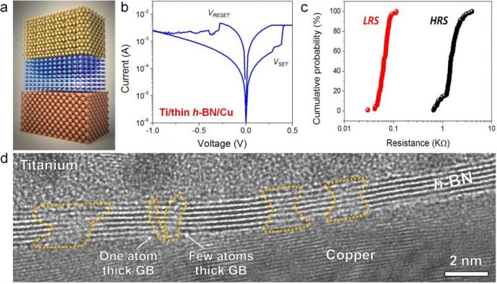 (a) Schematic of a Ti/thin h-BN/Cu RRAM device. (b) Typical I-V curves in a Ti/thin h-BN/Cu RRAM device showing bipolar RS. (c) Cumulative distribution of the resistance per cycle in HRS and LRS read at 0.1 V. (d) Cross-sectional TEM image showing defective paths (GBs) through the h-BN. (Copyright Wiley-VCH 2017. Reproduced with permission from the authors.)
A promising strategy that has recently gained an increased amount of interest in both industry and academia is the use of two dimensional (2D) layered materials to enhance the capabilities of electronic devices.
In depth applications and knowledge of 2D insulators is still limited even though the research in 2D semiconducting and metallic materials is well established.
The research team headed by Dr. Mario Lanza, a Young 1000 Talent Professor born in Barcelona, Spain, and based in Soochow University, China, is a significant global effort to examine the properties of layered dielectrics. A family of resistive random access memories (RRAM) was engineered by Lanza and co-workers, in his recent Advanced Functional Materials paper.
This was achieved using multilayer hexagonal boron nitride (h-BN) as dielectric. The patented devices demonstrate the coexistence of developing free bipolar and threshold-type resistive switching (RS) with low operation voltages down to 0.4 V, promising retention times above 10 hours, and high current on/off ratios up to 1,000,000, as well as low device-to-device and cycle -to-cycle variability.
The RS is driven by the grain boundaries (GBs) in the polycrystalline h-BN stack, which enable the penetration of metallic ions from neighboring electrodes. It is possible to boost this reaction by the generation of B vacancies, which are extremely abundant at the GBs.
The collaborated effort of The Massachusetts Institute of Technology, Stanford University and Harvard University (among others) has led to the development of this investigation. The outcomes of this investigation could have significant implications on the production of digital electronic devices made from 2D materials.