Apr 4 2017
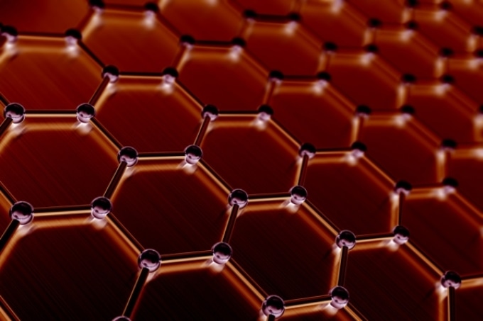 Researchers at MIT have found a way to make graphene with fewer wrinkles, and to iron out the wrinkles that do appear. They found each wafer exhibited uniform performance, meaning that electrons flowed freely across each wafer, at similar speeds, even across previously wrinkled regions. (Credit: MIT researchers)
Just like in a hair-raising thrill ride, electrons can move through graphene. Scientists have been aware for years that electrons can blitz through graphene close to the speed of light, much faster than they can move through silicon and other semiconducting materials.
Graphene, consequently, has been hyped as a potential successor to silicon, with the capacity to enable faster, highly efficient photonic and electronic devices.
However, producing pristine graphene — a single, very flat, extremely thin sheet of carbon atoms properly aligned and connected together like chickenwire — is very difficult. Conventional fabrication techniques repeatedly create wrinkles, which can disrupt an electron’s bullet-train movement, considerably restraining the electrical performance of graphene.
Recently, a team of MIT engineers have discovered a method to not only create graphene with fewer wrinkles, but also to iron out the wrinkles if they do appear. Once the fabrication and flattening out of the graphene was done, the engineers tested its electrical conductivity. They noticed that each wafer displayed uniform performance, suggesting that electrons flowed easily across each wafer, at similar speeds, even across formerly wrinkled portions.
In a research paper published today in the Proceedings of the National Academy of Sciences, the MIT team states that their processes effectively create wafer-scale, “single-domain” graphene — single layers of graphene that are even in both electronic performance and atomic arrangement.
For graphene to play as a main semiconductor material for industry, it has to be single-domain, so that if you make millions of devices on it, the performance of the devices is the same in any location. Now we can really produce single-domain graphene at wafer scale.
Jeehwan Kim, MIT
Kim’s co-authors include Sanghoon Bae, Samuel Cruz, and Yunjo Kim from MIT, along with researchers from IBM, the University of California at Los Angeles, and Kyungpook National University in South Korea.
A patchwork of wrinkles
Manufacturing graphene involves a very common process called chemical vapor deposition (CVD), where carbon atoms are placed onto a crystalline substrate such as copper foil. After ensuring that the copper foil is uniformly coated with a single layer of carbon atoms, the researchers submerge the whole thing in acid to etch away the copper. A single sheet of graphene is what is finally left behind. The researchers then pull it out from the acid.
The CVD process creates somewhat large, macroscropic wrinkles in graphene because of the roughness of the underlying copper as well as the process of pulling the sheet out from the acid. The arrangement of carbon atoms is not even across the graphene, forming a “polycrystalline” state where graphene looks like an uneven, patchwork terrain, preventing electrons from flowing at unvarying rates.
In 2013, when working at IBM, Kim and his colleagues formulated a technique to fabricate single-crystalline graphene wafers, in which the alignment of carbon atoms is exactly the same across the entire wafer.
Instead of using CVD, his team created single-crystalline graphene using a silicon carbide wafer with an atomically smooth surface, although with minute, step-like wrinkles on the order of several nanometers. Then a process known as layer-resolved graphene transfer was used to peel off the topmost graphene from the silicon carbide wafer using a thin sheet of nickel.
Ironing charges
In their recent paper, Kim and his colleagues observed that the layer-resolved graphene transfer smoothens out the steps and minute wrinkles in silicon carbide-fabricated graphene. Prior to moving the layer of graphene onto a silicon wafer, the MIT team oxidized the silicon, forming a layer of silicon dioxide that naturally displays electrostatic charges. When the researchers then placed the graphene, the silicon dioxide successfully pulled graphene’s carbon atoms down onto the wafer, ironing out its steps and wrinkles.
Kim says this ironing technique would not have an effect on CVD-fabricated graphene, as the wrinkles produced via CVD are a lot larger, on the order of several microns.
“The CVD process creates wrinkles that are too high to be ironed out,” Kim notes. “For silicon carbide graphene, the wrinkles are just a few nanometers high, short enough to be flattened out.”
To examine if the flattened, single-crystalline graphene wafers were single-domain, the research team fabricated miniature transistors on numerous sites on each wafer, including across formerly wrinkled regions.
We measured electron mobility throughout the wafers, and their performance was comparable. What’s more, this mobility in ironed graphene is two times faster. So now we really have single-domain graphene, and its electrical quality is much higher [than graphene-attached silicon carbide].
Jeehwan Kim, MIT
Kim says that although some challenges to adapting graphene for use in electronics remains, the team’s results offer scientists a blueprint for how to consistently create pristine, wrinkle-free, single-domain graphene at wafer scale.
If you want to make any electronic device using graphene, you need to work with single-domain graphene. There’s still a long way to go to make an operational transistor out of graphene. But we can now show the community guidelines for how you can make single-crystalline, single-domain graphene.
Jeehwan Kim, MIT